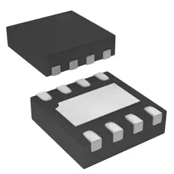
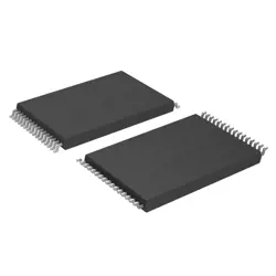
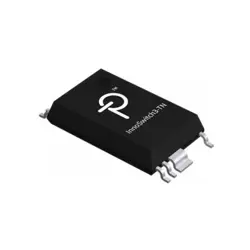
Bilder sind nur zur Referenz
10M02SCU169A7G
IC FPGA 130 I/O 169UBGA
- Hersteller
- Fr. Teil #10M02SCU169A7G
- Paket
- Datenblatt 10M02SCU169A7G DataSheet
- Auf Lager5465
100% Original und Neu
24 Stunden bereit zum Versand
365 Tage Garantie
RFQ & Erhalten Sie mehr Rabatte
Spezifikationen
| Series | MAX® 10 |
| Part Status | Active |
| DigiKey Programmable | Not Verified |
| Total RAM Bits | 110592 |
| Number of I/O | 130 |
| Voltage - Supply | 2.85V ~ 3.465V |
| Mounting Type | Surface Mount |
| Operating Temperature | -40°C ~ 125°C (TJ) |
| Package / Case | 169-LFBGA |
| Supplier Device Package | 169-UBGA (11x11) |
| Number of Logic Elements/Cells | 2000 |
| Number of LABs/CLBs | 125 |
Übersicht
Description
The MAX 10 series is notable for its low power consumption and built-in capabilities such as digital signal processing, allowing for efficient performance in tasks such as data communication, consumer electronics, and industrial applications. It also includes features like USB Blaster support and flash memory, enabling easier programming and configuration.
With a combination of programmability, high performance, and cost-effectiveness, the 10M02SCU169A7G is well-suited for prototyping and deploying designs in various computing environments.
Features
1. Logic Elements: It comprises a configurable fabric with 2,000 logic elements, allowing for versatile digital design and functionality.
2. Embedded Memory: The device includes up to 132 Kbits of embedded memory, facilitating efficient data storage and manipulation.
3. I/O Pins: It has 169 I/O pins, enabling extensive connectivity for external components and systems.
4. Operating Voltage: The FPGA operates at a voltage of 1.2V, which helps in power efficiency.
5. Speed Grade: It features a 7-speed grade, indicating the performance level suitable for various applications.
6. Configuration Options: The device supports multiple configuration methods, including JTAG and passive serial, allowing for flexible deployment.
7. Applications: Commonly used in automotive, industrial, and consumer electronics for tasks like signal processing, control systems, and more.
Overall, the 10M02SCU169A7G is designed for low to mid-range applications requiring programmable logic and efficient processing capabilities.
Package
Pinout
Key functions of the 10M02SCU169A7G include:
1. Logic Elements: It contains a configurable number of logic elements suitable for implementing complex logic functions.
2. I/O Pins: Supports multiple I/O standards for interfacing with peripheral devices.
3. RAM Blocks: Includes embedded memory blocks for efficient data storage and manipulation.
4. DSP Blocks: Provides dedicated resources for digital signal processing tasks.
5. Embedded JTAG: For debugging and programming purposes.
6. User Flash Memory: Allows for non-volatile storage of user data.
This FPGA is ideal for low to mid-range applications that require flexibility and configurability.
Manufacturer
Application
Equivalent
1. LatticeECP3-70
2. Xilinx Artix-7 (e.g., XC7A35T)
3. Microsemi SmartFusion2 (e.g., M2S010)
4. Cypress PSoC 5LP
Check specific requirements and compatibility for your applications when selecting an equivalent product.
Versand
VersandmethodenWir
bieten Sie globale Versanddienstleistungen durch DHL, FedEx, TNT, UPS oder einen anderen Spediteur Ihrer Wahl.
Versandgebührenreferenz (DHL/FedEx):
DHL: Versandkosten reichen von $25-$45 (0.5kg), mit einer geschätzten Lieferzeit von 2-5 Werktagen.
von FedEx: Versandkosten reichen von $25-$40 (0.5kg), mit einer geschätzten Lieferzeit von 3-7 Werktagen.
UPS: Versandkosten reichen von $25-$45 (0.5kg), mit einer geschätzten Lieferzeit von 3-7 Werktagen.
TNT: Versandkosten reichen von $25-$65 (0.5kg), mit einer geschätzten Lieferzeit von 3-7 Werktagen.
EMS: Versandkosten reichen von $30-$50 (0.5kg), mit einer geschätzten Lieferzeit von 7-15 Werktagen.
Registrierte Luftpost: Versandkosten sind $ 2- $ 4 (0,1 kg), mit einer geschätzten Lieferzeit von 5-20 Werktagen.
Zahlungen
Payment Methods
Die Zahlungsfrist ist 100% Prepaid.
Derzeit akzeptieren wir nur die folgenden Zahlungsmethoden:
1. PayPal
2. Kredit- / Debitkarte
3. Überweisung
Ähnliche
-
![MX25V16066M1I02]() MX25V16066M1I02
MX25V16066M1I02
Macronix
-
![MX25R3235FZNIL0]() MX25R3235FZNIL0
MX25R3235FZNIL0
Macronix
-
![MX25R6435FBDIL0]() MX25R6435FBDIL0
MX25R6435FBDIL0
Macronix
-
![MX25L25673GMI-08G]() MX25L25673GMI-08G
MX25L25673GMI-08G
Macronix
-
![MX25L25673GMI-10G]() MX25L25673GMI-10G
MX25L25673GMI-10G
Macronix
-
![MX25U25643GZNI00]() MX25U25643GZNI00
MX25U25643GZNI00
Macronix
-
![MX25U3232FZBI02]() MX25U3232FZBI02
MX25U3232FZBI02
Macronix
-
![MX25U6435FM2I-10G]() MX25U6435FM2I-10G
MX25U6435FM2I-10G
Macronix
-
![MX25L12833FM2I-10G]() MX25L12833FM2I-10..
MX25L12833FM2I-10..
Macronix
-
![MX29F040CTI-70G]() MX29F040CTI-70G
MX29F040CTI-70G
Macronix
-
![MX25L1006EMI-10G]() MX25L1006EMI-10G
MX25L1006EMI-10G
Macronix
-
![MX66U1G45GMI00]() MX66U1G45GMI00
MX66U1G45GMI00
Macronix