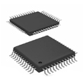
Bilder sind nur zur Referenz
10M04SCE144C8G
IC FPGA 101 I/O 144EQFP
- Hersteller
- Fr. Teil #10M04SCE144C8G
- Paket 144-LQFPExposedPad
- Datenblatt
- Auf Lager3511
100% Original und Neu
24 Stunden bereit zum Versand
365 Tage Garantie
RFQ & Erhalten Sie mehr Rabatte
Spezifikationen
| Package | Tray |
| Series | MAX® 10 |
| ProductStatus | Active |
| NumberofLABs/CLBs | 250 |
| NumberofLogicElements/Cells | 4000 |
| TotalRAMBits | 193536 |
| NumberofI/O | 101 |
| Voltage-Supply | 2.85V ~ 3.465V |
| MountingType | Surface Mount |
| OperatingTemperature | 0°C ~ 85°C (TJ) |
| Package/Case | 144-LQFP Exposed Pad |
Übersicht
Description
Key features of the 10M04SCE144C8G include:
- A capacity of approximately 4,000 logic elements.
- 144 pins, allowing for multiple I/O connections.
- C8G signifies a specific package type and temperature grade.
- The device is optimized for low power consumption, making it suitable for battery-operated or thermal-sensitive applications.
The FPGA can be programmed to implement custom hardware functions, enabling flexible design solutions across various industries.
Features
1. Logic Elements: It offers 4,608 logic elements, enabling flexible digital logic design.
2. Memory: Integrated with up to 160 Kbits of embedded memory, suitable for data storage and caching.
3. I/O Pins: Contains 144 I/O pins, supporting various communication protocols for interfacing.
4. Low Power: Designed for low power consumption, making it ideal for battery-operated devices.
5. Configuration Options: Supports multiple configuration methods, including JTAG and passive serial.
6. Single Supply Voltage: Operates at a single supply voltage of 1.2V to 3.6V, simplifying power management.
7. Embedded DSP Blocks: Includes dedicated DSP blocks for efficient digital signal processing tasks.
Overall, the 10M04SCE144C8G is suitable for applications requiring flexibility, compact design, and low power consumption in digital logic implementations.
Package
Pinout
The functions of its pins include:
- I/O pins: Configurable for various digital input/output operations, supporting standard logic levels.
- Power supply pins: Provide power to the FPGA core and I/O banks.
- Configuration pins: Used for programming the FPGA on power-up, including JTAG and dedicated configuration modes.
- Clock pins: Support external clock inputs for timing and synchronization.
- Ground pins: Common ground connections for stability.
The device is designed for applications requiring moderate logic density, and it offers features like embedded memory and DSP blocks. The specific functions of each pin can be referenced in the device's datasheet.
Manufacturer
Application
Equivalent
Versand
VersandmethodenWir
bieten Sie globale Versanddienstleistungen durch DHL, FedEx, TNT, UPS oder einen anderen Spediteur Ihrer Wahl.
Versandgebührenreferenz (DHL/FedEx):
DHL: Versandkosten reichen von $25-$45 (0.5kg), mit einer geschätzten Lieferzeit von 2-5 Werktagen.
von FedEx: Versandkosten reichen von $25-$40 (0.5kg), mit einer geschätzten Lieferzeit von 3-7 Werktagen.
UPS: Versandkosten reichen von $25-$45 (0.5kg), mit einer geschätzten Lieferzeit von 3-7 Werktagen.
TNT: Versandkosten reichen von $25-$65 (0.5kg), mit einer geschätzten Lieferzeit von 3-7 Werktagen.
EMS: Versandkosten reichen von $30-$50 (0.5kg), mit einer geschätzten Lieferzeit von 7-15 Werktagen.
Registrierte Luftpost: Versandkosten sind $ 2- $ 4 (0,1 kg), mit einer geschätzten Lieferzeit von 5-20 Werktagen.
Zahlungen
Payment Methods
Die Zahlungsfrist ist 100% Prepaid.
Derzeit akzeptieren wir nur die folgenden Zahlungsmethoden:
1. PayPal
2. Kredit- / Debitkarte
3. Überweisung
Ähnliche
-
![MX25L3233FM1I-08Q]() MX25L3233FM1I-08Q
Macronix
-
![MX25V1635FZNQ03]() MX25V1635FZNQ03
Macronix
-
![MX66U1G45GXDI00]() MX66U1G45GXDI00
Macronix
-
![MX25V16066M1I02]() MX25V16066M1I02
Macronix
-
![MX30LF2G28AD-TI]() MX30LF2G28AD-TI
Macronix
-
![MX29GL512FHXFI-11G]() MX29GL512FHXFI-11..
Macronix
-
![MX25U25643GZNI00]() MX25U25643GZNI00
Macronix
-
![MX25V1635FM2I]() MX25V1635FM2I
Macronix
-
![MX25L6433FM2I-08G]() MX25L6433FM2I-08G
Macronix
-
![MX25U6435FM2I-10G]() MX25U6435FM2I-10G
Macronix
-
![MX25L12833FM2I-10G]() MX25L12833FM2I-10..
Macronix
-
![MX29F040CQI-70G]() MX29F040CQI-70G
Macronix