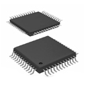
Bilder sind nur zur Referenz
10M25SCE144C8G
IC FPGA 101 I/O 144EQFP
- Hersteller
- Fr. Teil #10M25SCE144C8G
- Paket
- Datenblatt
- Auf Lager2239
100% Original und Neu
24 Stunden bereit zum Versand
365 Tage Garantie
RFQ & Erhalten Sie mehr Rabatte
Spezifikationen
| Series | MAX® 10 |
| Part Status | Active |
| DigiKey Programmable | Not Verified |
| Total RAM Bits | 691200 |
| Number of I/O | 101 |
| Voltage - Supply | 2.85V ~ 3.465V |
| Mounting Type | Surface Mount |
| Operating Temperature | 0°C ~ 85°C (TJ) |
| Package / Case | 144-LQFP Exposed Pad |
| Supplier Device Package | 144-EQFP (20x20) |
| Number of Logic Elements/Cells | 25000 |
| Number of LABs/CLBs | 1563 |
Übersicht
Description
Key features include built-in flash memory, digital signal processing capabilities, and support for various communication protocols. Its compact design allows for efficient integration into embedded systems, while the 8G indicates the package type and pin count—144 pins in total. The device is programmable, enabling developers to customize functionality as per project requirements.
The 10M25SCE144C8G is ideal for designers seeking a balance between cost-effectiveness and performance, offering robust support for development tools such as Intel Quartus for seamless programming and debugging.
Features
- Logic Elements: 25,000 logic elements for complex digital designs.
- I/O Pins: 144 I/O pins supporting various I/O standards, suitable for diverse applications.
- Memory: On-chip RAM blocks for efficient data storage and processing.
- DSP Blocks: Integrated DSP blocks for high-performance signal processing tasks.
- Power Efficiency: Low static and dynamic power consumption, making it suitable for power-sensitive applications.
- Configuration: Flexible configuration options, allowing for quick reprogramming and prototyping.
- Development Tools: Compatible with Intel's Quartus Prime software for design implementation and testing.
This FPGA is ideal for applications in communications, automotive, industrial, and consumer electronics, providing a balance of performance and versatility.
Package
Pinout
The main functions of these pins include:
- I/O Operations: Configurable as input, output, or bidirectional signals for interfacing with other devices.
- Power: Dedicated pins for power supply and ground connections.
- Configuration: Pins for configuring the FPGA, including JTAG programming support.
- Clock Inputs: Pins for receiving clock signals to drive internal logic.
- User-defined Functions: Many pins can be repurposed for specific application needs based on user designs.
Overall, the 10M25SCE144C8G is designed for flexibility and ease of integration in various electronic applications.
Manufacturer
Application
Equivalent
Versand
VersandmethodenWir
bieten Sie globale Versanddienstleistungen durch DHL, FedEx, TNT, UPS oder einen anderen Spediteur Ihrer Wahl.
Versandgebührenreferenz (DHL/FedEx):
DHL: Versandkosten reichen von $25-$45 (0.5kg), mit einer geschätzten Lieferzeit von 2-5 Werktagen.
von FedEx: Versandkosten reichen von $25-$40 (0.5kg), mit einer geschätzten Lieferzeit von 3-7 Werktagen.
UPS: Versandkosten reichen von $25-$45 (0.5kg), mit einer geschätzten Lieferzeit von 3-7 Werktagen.
TNT: Versandkosten reichen von $25-$65 (0.5kg), mit einer geschätzten Lieferzeit von 3-7 Werktagen.
EMS: Versandkosten reichen von $30-$50 (0.5kg), mit einer geschätzten Lieferzeit von 7-15 Werktagen.
Registrierte Luftpost: Versandkosten sind $ 2- $ 4 (0,1 kg), mit einer geschätzten Lieferzeit von 5-20 Werktagen.
Zahlungen
Payment Methods
Die Zahlungsfrist ist 100% Prepaid.
Derzeit akzeptieren wir nur die folgenden Zahlungsmethoden:
1. PayPal
2. Kredit- / Debitkarte
3. Überweisung
Ähnliche
-
![MX29F400CBTI-70G]() MX29F400CBTI-70G
Macronix
-
![MX25V5126FM1I]() MX25V5126FM1I
Macronix
-
![MX25V4035FZUI]() MX25V4035FZUI
Macronix
-
![MX25R6435FBDIL0]() MX25R6435FBDIL0
Macronix
-
![MX25L25673GMI-08G]() MX25L25673GMI-08G
Macronix
-
![MX29GL512FHXFI-11G]() MX29GL512FHXFI-11..
Macronix
-
![MX25R1635FZUIH0]() MX25R1635FZUIH0
Macronix
-
![MX25V1635FM2I]() MX25V1635FM2I
Macronix
-
![MX25U6435FM2I-10G]() MX25U6435FM2I-10G
Macronix
-
![MX25L25645GXDI-08G]() MX25L25645GXDI-08..
Macronix
-
![MX29F800CBTI-70G]() MX29F800CBTI-70G
Macronix
-
![MX25U51245GZ4I00]() MX25U51245GZ4I00
Macronix