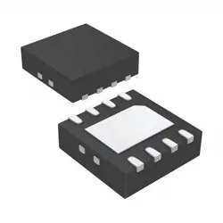
Bilder sind nur zur Referenz
5M2210ZF256C5N
IC CPLD 1700MC 7NS 256FBGA
- Hersteller
- Fr. Teil #5M2210ZF256C5N
- Paket FBGA-256
- Datenblatt
- Auf Lager7152
100% Original und Neu
24 Stunden bereit zum Versand
365 Tage Garantie
RFQ & Erhalten Sie mehr Rabatte
Spezifikationen
| Package | Tray |
| Series | MAX® V |
| ProductStatus | Active |
| ProgrammableType | In System Programmable |
| DelayTimetpd(1)Max | 7 ns |
| VoltageSupply-Internal | 1.71V ~ 1.89V |
| NumberofLogicElements/Blocks | 2210 |
| NumberofMacrocells | 1700 |
| NumberofI/O | 203 |
| OperatingTemperature | 0°C ~ 85°C (TJ) |
| MountingType | Surface Mount |
| Package/Case | 256-LBGA |
Übersicht
Description
Key specifications include:
- Logic Elements (LEs): The 5M2210ZF256C5N typically contains around 2,210 logic elements, allowing for complex digital designs.
- Memory: It includes embedded memory blocks for efficient data storage and processing.
- I/O Pins: The device supports multiple I/O pins for interfacing with external devices.
- Operating Voltage: It operates at a low voltage of around 1.2V to 3.3V, enhancing energy efficiency.
- Configuration: The FPGA can be configured through various methods, including JTAG and serial configuration.
Overall, the 5M2210ZF256C5N is designed for flexibility and efficiency, enabling designers to implement custom digital circuits tailored to specific project needs.
Features
1. Capacity: It offers 22,000 logic elements, making it suitable for various applications.
2. Embedded Memory: Supports up to 1.1 Mbits of embedded memory, allowing for efficient data storage and manipulation.
3. I/O Support: Provides 256 user I/O pins, enabling extensive connectivity options.
4. Operating Voltage: Features a low operating voltage of 1.2V, which contributes to lower power consumption.
5. On-chip Flash: Integrates on-chip flash memory for configuration and design flexibility.
6. Analog Features: Includes analog-to-digital converters (ADCs) for mixed-signal processing capabilities.
7. High-speed Performance: Supports high-speed serial interfaces, including SPI and I2C, for versatile communication options.
8. Development Tools: Compatible with Intel's Quartus Prime software for design and simulation.
This combination of features makes the 5M2210ZF256C5N ideal for various applications, including automotive, industrial, and consumer electronics.
Package
Pinout
The primary functions of the 5M2210ZF256C5N include digital logic implementation, signal processing, and various configurable I/O operations. It supports a variety of interfaces, including GPIO, I2C, SPI, and UART, allowing for versatile connectivity options in embedded systems. The device is designed for applications in fields such as industrial automation, automotive, and consumer electronics.
Additionally, it features on-chip memory resources and is optimized for low power consumption, making it ideal for cost-sensitive applications.
Manufacturer
Application
Equivalent
Versand
VersandmethodenWir
bieten Sie globale Versanddienstleistungen durch DHL, FedEx, TNT, UPS oder einen anderen Spediteur Ihrer Wahl.
Versandgebührenreferenz (DHL/FedEx):
DHL: Versandkosten reichen von $25-$45 (0.5kg), mit einer geschätzten Lieferzeit von 2-5 Werktagen.
von FedEx: Versandkosten reichen von $25-$40 (0.5kg), mit einer geschätzten Lieferzeit von 3-7 Werktagen.
UPS: Versandkosten reichen von $25-$45 (0.5kg), mit einer geschätzten Lieferzeit von 3-7 Werktagen.
TNT: Versandkosten reichen von $25-$65 (0.5kg), mit einer geschätzten Lieferzeit von 3-7 Werktagen.
EMS: Versandkosten reichen von $30-$50 (0.5kg), mit einer geschätzten Lieferzeit von 7-15 Werktagen.
Registrierte Luftpost: Versandkosten sind $ 2- $ 4 (0,1 kg), mit einer geschätzten Lieferzeit von 5-20 Werktagen.
Zahlungen
Payment Methods
Die Zahlungsfrist ist 100% Prepaid.
Derzeit akzeptieren wir nur die folgenden Zahlungsmethoden:
1. PayPal
2. Kredit- / Debitkarte
3. Überweisung
Ähnliche
-
![MX25V1635FZNQ03]() MX25V1635FZNQ03
MX25V1635FZNQ03
Macronix
-
![MX25V4035FZUI]() MX25V4035FZUI
MX25V4035FZUI
Macronix
-
![MX25V16066M2I02]() MX25V16066M2I02
MX25V16066M2I02
Macronix
-
![MX30LF2G28AD-TI]() MX30LF2G28AD-TI
MX30LF2G28AD-TI
Macronix
-
![MX25L8035EM2I-10G]() MX25L8035EM2I-10G
MX25L8035EM2I-10G
Macronix
-
![MX25R6435FBDIL0]() MX25R6435FBDIL0
MX25R6435FBDIL0
Macronix
-
![MX25U6435FM2I-10G]() MX25U6435FM2I-10G
MX25U6435FM2I-10G
Macronix
-
![MX25L12833FM2I-10G]() MX25L12833FM2I-10..
MX25L12833FM2I-10..
Macronix
-
![MX25L12833FZ2I-10G]() MX25L12833FZ2I-10..
MX25L12833FZ2I-10..
Macronix
-
![MX25L12833FZNI-10G]() MX25L12833FZNI-10..
MX25L12833FZNI-10..
Macronix
-
![MX25U25645GXDI00]() MX25U25645GXDI00
MX25U25645GXDI00
Macronix
-
![MX29LV160DTTI-70G]() MX29LV160DTTI-70G
MX29LV160DTTI-70G
Macronix