
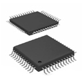
Bilder sind nur zur Referenz
74HC2G04GW
- Hersteller
- Fr. Teil #74HC2G04GW
- Paket
- Datenblatt
- Auf Lager8313
100% Original und Neu
24 Stunden bereit zum Versand
365 Tage Garantie
RFQ & Erhalten Sie mehr Rabatte
Spezifikationen
| Brand | Nexperia |
Übersicht
Description
This component is housed in a compact TSSOP-8 package, making it suitable for space-constrained designs. Each inverter has a standard push-pull output configuration, ensuring fast switching speeds. The typical propagation delay is around 7 ns at a 5V supply, making it suitable for high-speed applications.
The 74HC2G04GW is compatible with TTL inputs, allowing it to interface easily with other digital circuits. It is commonly used in signal inversion tasks, waveform shaping, and other applications requiring logic level inversion. Additionally, the component is characterized by a high degree of thermal stability and robustness, with ESD protection mechanisms ensuring reliability in harsh environments.
Features
1. Voltage Range: Operates over a wide voltage range from 2V to 6V, making it suitable for various applications.
2. Low Power Consumption: Designed for low power usage due to its CMOS technology.
3. High Speed: Offers fast switching times, ensuring quick response in digital circuits.
4. Input Levels: Compatible with TTL input levels, which allows it to interface with other TTL devices.
5. Output Capability: Provides standard CMOS output drive, capable of driving inputs of other gates effectively.
6. Package: Available in a small SOT363 package, which is suitable for space-constrained applications.
7. Temperature Range: Functions over a wide temperature range, typically from -40°C to +125°C, making it robust for various environmental conditions.
8. Latch-up Performance: High immunity to latch-up, ensuring reliable operation.
These features make the 74HC2G04GW ideal for use in digital electronics where inversion of signal levels is required in a compact form factor.
Package
Pinout
Here’s a concise description of the pin functions:
1. Pin 1: Input A1 – First inverter input.
2. Pin 2: Output Y1 – First inverter output (inverted signal of A1).
3. Pin 3: Input A2 – Second inverter input.
4. Pin 4: Ground (GND) – Connects to the ground of the circuit.
5. Pin 5: Output Y2 – Second inverter output (inverted signal of A2).
6. Pin 6: Input A3 – Third inverter input.
7. Pin 7: Output Y3 – Third inverter output (inverted signal of A3).
8. Pin 8: Supply Voltage (VCC) – Connects to the positive power supply.
This dual inverter is useful in digital circuits where signal inversion is required, ensuring minimal delay and low power consumption thanks to the use of CMOS technology.
Manufacturer
Application
Equivalent
Versand
VersandmethodenWir
bieten Sie globale Versanddienstleistungen durch DHL, FedEx, TNT, UPS oder einen anderen Spediteur Ihrer Wahl.
Versandgebührenreferenz (DHL/FedEx):
DHL: Versandkosten reichen von $25-$45 (0.5kg), mit einer geschätzten Lieferzeit von 2-5 Werktagen.
von FedEx: Versandkosten reichen von $25-$40 (0.5kg), mit einer geschätzten Lieferzeit von 3-7 Werktagen.
UPS: Versandkosten reichen von $25-$45 (0.5kg), mit einer geschätzten Lieferzeit von 3-7 Werktagen.
TNT: Versandkosten reichen von $25-$65 (0.5kg), mit einer geschätzten Lieferzeit von 3-7 Werktagen.
EMS: Versandkosten reichen von $30-$50 (0.5kg), mit einer geschätzten Lieferzeit von 7-15 Werktagen.
Registrierte Luftpost: Versandkosten sind $ 2- $ 4 (0,1 kg), mit einer geschätzten Lieferzeit von 5-20 Werktagen.
Zahlungen
Payment Methods
Die Zahlungsfrist ist 100% Prepaid.
Derzeit akzeptieren wir nur die folgenden Zahlungsmethoden:
1. PayPal
2. Kredit- / Debitkarte
3. Überweisung
Ähnliche
-
![MX25R8035FM1IL0]() MX25R8035FM1IL0
Macronix
-
![MX25L3233FM1I-08Q]() MX25L3233FM1I-08Q
Macronix
-
![MX25V1635FZNI]() MX25V1635FZNI
Macronix
-
![MX25V1635FZNQ03]() MX25V1635FZNQ03
Macronix
-
![MX66U1G45GXDI00]() MX66U1G45GXDI00
Macronix
-
![MX25L8035EM2I-10G]() MX25L8035EM2I-10G
Macronix
-
![MX25L25673GMI-08G]() MX25L25673GMI-08G
Macronix
-
![MX25U25643GZNI00]() MX25U25643GZNI00
Macronix
-
![MX25L2006EM1I-12G]() MX25L2006EM1I-12G
Macronix
-
![MX25L6433FM2I-08G]() MX25L6433FM2I-08G
Macronix
-
![MX25U6435FM2I-10G]() MX25U6435FM2I-10G
Macronix
-
![MX25L12833FM2I-10G]() MX25L12833FM2I-10..
Macronix


