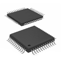
Bilder sind nur zur Referenz
74HC2G17GW
Nexperia
- Hersteller
- Fr. Teil #74HC2G17GW
- Paket
- Datenblatt
- Auf Lager16352
100% Original und Neu
24 Stunden bereit zum Versand
365 Tage Garantie
RFQ & Erhalten Sie mehr Rabatte
Spezifikationen
Übersicht
Description
The Schmitt-trigger design allows it to handle slow input signals and mitigate signal distortion, ensuring clean output transitions. The 74HC2G17GW operates over a voltage range of 2V to 6V, accommodating various logic levels. It is available in a compact SOT-23 package, making it suitable for space-constrained applications.
Typical uses include driving LEDs, interfacing with microcontrollers, and cleaning up noisy signals in communication lines. The device has a low power dissipation, enhancing battery life in portable applications. Overall, the 74HC2G17GW is an essential component for reliable digital logic operations in modern electronic designs.
Features
1. Dual Functionality: It provides two independent buffer/inverter circuits, enhancing versatility in applications.
2. Schmitt Trigger Inputs: The Schmitt-trigger design offers improved noise immunity and defines clean switching thresholds, making it suitable for transitioning slow signals.
3. High Speed: Operates at high speeds, with typical propagation delays of 7 ns at 5V, enabling fast signal processing.
4. Wide Voltage Range: It operates within a supply voltage range of 2V to 6V, accommodating various logic levels.
5. Low Power Consumption: Consumes less power during operation, making it ideal for battery-powered devices.
6. Wide Operating Temperature: Suitable for a broad temperature range, typically from -40°C to +125°C.
7. Surface Mount Package: Available in the SOT-23-5 package, facilitating compact designs and efficient PCB layout.
These features make the 74HC2G17GW well-suited for digital signal conditioning, interfacing, and logic-level shifting in various electronic applications.
Package
Pinout
Pin Functions:
1. Pin 1 (A1): Input for Buffer 1
2. Pin 2 (Y1): Output for Buffer 1
3. Pin 3 (A2): Input for Buffer 2
4. Pin 4 (Y2): Output for Buffer 2
5. Pin 5 (GND): Ground connection
The device is designed to provide clean transitions between logic levels, improving noise immunity and allowing for slow input signal changes. It operates within a supply voltage range of 2V to 6V, making it suitable for various digital applications.
Manufacturer
Application
Equivalent
1. 74HCT2G17 (TTL compatible)
2. 74LVC2G17 (low-voltage CMOS)
3. 74AHC2G17 (high-speed CMOS)
4. 74AC2G17 (advanced CMOS)
Ensure compatibility with your specific voltage and logic level requirements when selecting alternatives.
Versand
VersandmethodenWir
bieten Sie globale Versanddienstleistungen durch DHL, FedEx, TNT, UPS oder einen anderen Spediteur Ihrer Wahl.
Versandgebührenreferenz (DHL/FedEx):
DHL: Versandkosten reichen von $25-$45 (0.5kg), mit einer geschätzten Lieferzeit von 2-5 Werktagen.
von FedEx: Versandkosten reichen von $25-$40 (0.5kg), mit einer geschätzten Lieferzeit von 3-7 Werktagen.
UPS: Versandkosten reichen von $25-$45 (0.5kg), mit einer geschätzten Lieferzeit von 3-7 Werktagen.
TNT: Versandkosten reichen von $25-$65 (0.5kg), mit einer geschätzten Lieferzeit von 3-7 Werktagen.
EMS: Versandkosten reichen von $30-$50 (0.5kg), mit einer geschätzten Lieferzeit von 7-15 Werktagen.
Registrierte Luftpost: Versandkosten sind $ 2- $ 4 (0,1 kg), mit einer geschätzten Lieferzeit von 5-20 Werktagen.
Zahlungen
Payment Methods
Die Zahlungsfrist ist 100% Prepaid.
Derzeit akzeptieren wir nur die folgenden Zahlungsmethoden:
1. PayPal
2. Kredit- / Debitkarte
3. Überweisung
Ähnliche
-
![MX25V1635FZNQ03]() MX25V1635FZNQ03
Macronix
-
![MX66U1G45GXDI00]() MX66U1G45GXDI00
Macronix
-
![MX25V5126FM1I]() MX25V5126FM1I
Macronix
-
![MX25V4035FZUI]() MX25V4035FZUI
Macronix
-
![MX25V16066M1I02]() MX25V16066M1I02
Macronix
-
![MX25R6435FBDIL0]() MX25R6435FBDIL0
Macronix
-
![MX29GL512FHXFI-11G]() MX29GL512FHXFI-11..
Macronix
-
![MX25R1635FZUIH0]() MX25R1635FZUIH0
Macronix
-
![MX25V1635FM2I]() MX25V1635FM2I
Macronix
-
![MX25L12833FM2I-10G]() MX25L12833FM2I-10..
Macronix
-
![MX25L12833FZ2I-10G]() MX25L12833FZ2I-10..
Macronix
-
![MX29LV640ETTI-70G]() MX29LV640ETTI-70G
Macronix