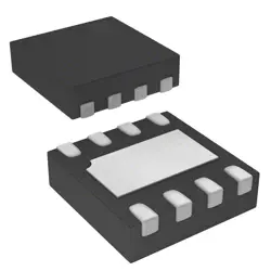
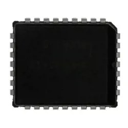
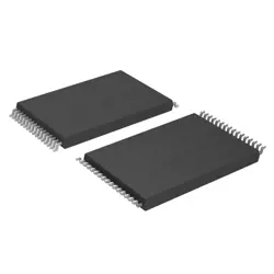
Bilder sind nur zur Referenz
74HC595
IC 74HC595 8-Bit Shift Register
- Hersteller
- Fr. Teil #74HC595
- Paket
- Datenblatt
- Auf Lager6832
100% Original und Neu
24 Stunden bereit zum Versand
365 Tage Garantie
RFQ & Erhalten Sie mehr Rabatte
Spezifikationen
| Series | 74HC |
| Part Status | Active |
| Mounting Type | Through Hole |
Übersicht
Description
The 74HC595 operates using three primary pins: the data input (SER), a clock pin (SRCLK), and a latch pin (RCLK). Data is shifted in on the rising edge of the clock signal, and the output state can be latched to the output pins using the latch pin. The chip also features cascading capability, allowing multiple 74HC595 chips to be connected together to increase the number of outputs.
This IC is widely used in LED displays, shift registers, and other applications requiring efficient control of multiple outputs while minimizing the number of pins used on a microcontroller. Its ease of use and versatility make it a popular choice among hobbyists and professionals alike.
Features
1. 8-bit Storage: Stores 8 bits of data, allowing control of multiple outputs with fewer microcontroller pins.
2. Serial In, Parallel Out: Data is shifted in serially and can be output in parallel format.
3. Cascade Capability: Multiple 74HC595 chips can be connected in series for increased output (up to 64 bits with 8 chips).
4. Latch Functionality: Has a separate latch to hold outputs stable while new data is shifted in.
5. High-Speed Operation: Operates at high speeds (up to 100 MHz), suitable for fast applications.
6. 3-State Outputs: Outputs can be set to a high impedance state, allowing for easy interfacing with other devices.
7. Wide Voltage Range: Operates at 2V to 6V, making it versatile for various projects.
These features make the 74HC595 ideal for applications in LED driving, multiplexing, and other digital control tasks.
Package
Pinout
1. VCC (Pin 1): Power supply.
2. GND (Pin 8): Ground.
3. DS (Pin 2): Serial data input.
4. OE (Pin 3): Output enable (active low).
5. ST_CP (Pin 4): Storage register clock (latch data to outputs).
6. SH_CP (Pin 11): Shift register clock (shifts data into the register).
7. MR (Pin 10): Master reset (active low, resets the register).
8. Q0-Q7 (Pins 15-7): Parallel output pins (Q0 is the first bit shifted in).
The device allows for easy expansion of output pins using a serial data interface, making it ideal for driving LEDs and other peripherals.
Manufacturer
Application
Equivalent
Versand
VersandmethodenWir
bieten Sie globale Versanddienstleistungen durch DHL, FedEx, TNT, UPS oder einen anderen Spediteur Ihrer Wahl.
Versandgebührenreferenz (DHL/FedEx):
DHL: Versandkosten reichen von $25-$45 (0.5kg), mit einer geschätzten Lieferzeit von 2-5 Werktagen.
von FedEx: Versandkosten reichen von $25-$40 (0.5kg), mit einer geschätzten Lieferzeit von 3-7 Werktagen.
UPS: Versandkosten reichen von $25-$45 (0.5kg), mit einer geschätzten Lieferzeit von 3-7 Werktagen.
TNT: Versandkosten reichen von $25-$65 (0.5kg), mit einer geschätzten Lieferzeit von 3-7 Werktagen.
EMS: Versandkosten reichen von $30-$50 (0.5kg), mit einer geschätzten Lieferzeit von 7-15 Werktagen.
Registrierte Luftpost: Versandkosten sind $ 2- $ 4 (0,1 kg), mit einer geschätzten Lieferzeit von 5-20 Werktagen.
Zahlungen
Payment Methods
Die Zahlungsfrist ist 100% Prepaid.
Derzeit akzeptieren wir nur die folgenden Zahlungsmethoden:
1. PayPal
2. Kredit- / Debitkarte
3. Überweisung
Ähnliche
-
![MX25R8035FM1IL0]() MX25R8035FM1IL0
MX25R8035FM1IL0
Macronix
-
![MX25V1635FZNI]() MX25V1635FZNI
MX25V1635FZNI
Macronix
-
![MX29F400CBTI-70G]() MX29F400CBTI-70G
MX29F400CBTI-70G
Macronix
-
![MX25V16066M1I02]() MX25V16066M1I02
MX25V16066M1I02
Macronix
-
![MX29GL512FHXFI-11G]() MX29GL512FHXFI-11..
MX29GL512FHXFI-11..
Macronix
-
![MX25R1635FZUIH0]() MX25R1635FZUIH0
MX25R1635FZUIH0
Macronix
-
![MX25V1635FM2I]() MX25V1635FM2I
MX25V1635FM2I
Macronix
-
![MX25L12833FZ2I-10G]() MX25L12833FZ2I-10..
MX25L12833FZ2I-10..
Macronix
-
![MX25U25645GXDI00]() MX25U25645GXDI00
MX25U25645GXDI00
Macronix
-
![MX29F040CQI-70G]() MX29F040CQI-70G
MX29F040CQI-70G
Macronix
-
![MX29F040CTI-70G]() MX29F040CTI-70G
MX29F040CTI-70G
Macronix
-
![MX29F800CBTI-70G]() MX29F800CBTI-70G
MX29F800CBTI-70G
Macronix