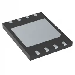
Bilder sind nur zur Referenz
74LVC1G126GW
Buffers & Line Drivers
- Hersteller
- Fr. Teil #74LVC1G126GW
- Paket
- Datenblatt
- Auf Lager9210
100% Original und Neu
24 Stunden bereit zum Versand
365 Tage Garantie
RFQ & Erhalten Sie mehr Rabatte
Spezifikationen
Übersicht
Description
Key specifications include a supply voltage range of 1.65V to 5.5V, making it suitable for various logic levels, including 3.3V and 5V systems. The device operates at high speeds with a propagation delay of around 3.5 ns at 3.3V. The input and output are compatible with standard LVC logic levels, ensuring broad usability in digital designs.
The package type, GW, indicates a small footprint, which is ideal for space-constrained applications. Typical use cases include signal buffering, level shifting, and bus driving in microcontroller and FPGA interfaces. Overall, the 74LVC1G126GW is a versatile component for modern electronic designs requiring efficient signal management.
Features
1. Voltage Range: Operates from 1.65V to 5.5V, making it suitable for various low-voltage applications.
2. Low Power Consumption: Offers low static and dynamic power consumption, ideal for battery-operated devices.
3. High-Speed Operation: Supports fast switching times, enhancing performance in high-speed applications.
4. Three-State Outputs: The outputs can be placed in a high-impedance state, allowing for bus-oriented applications and reducing loading on shared lines.
5. Input Compatibility: Compatible with TTL (Transistor-Transistor Logic) levels, enabling easy interfacing with other logic families.
6. ESD Protection: Provides robust electrostatic discharge protection, ensuring reliability in harsh environments.
7. Small Package: Available in compact packages (e.g., SC-70), facilitating space-saving designs.
This versatile device is widely used in signal buffering, level shifting, and interfacing applications.
Package
Pinout
1. A (Input): This is the data input pin.
2. OE (Output Enable): Controls the output state. When enabled, the output reflects the input state; when disabled, the output is in high-impedance.
3. Y (Output): This is the buffered output pin that reflects the input state when the output is enabled.
4. VCC (Power Supply): The supply voltage pin, typically ranging from 1.65V to 5.5V.
5. GND (Ground): The ground connection pin.
The device is commonly used in digital circuits for signal buffering and level shifting, providing a way to control the flow of signals while ensuring the output can be disabled when not in use.
Manufacturer
Application
Equivalent
Versand
VersandmethodenWir
bieten Sie globale Versanddienstleistungen durch DHL, FedEx, TNT, UPS oder einen anderen Spediteur Ihrer Wahl.
Versandgebührenreferenz (DHL/FedEx):
DHL: Versandkosten reichen von $25-$45 (0.5kg), mit einer geschätzten Lieferzeit von 2-5 Werktagen.
von FedEx: Versandkosten reichen von $25-$40 (0.5kg), mit einer geschätzten Lieferzeit von 3-7 Werktagen.
UPS: Versandkosten reichen von $25-$45 (0.5kg), mit einer geschätzten Lieferzeit von 3-7 Werktagen.
TNT: Versandkosten reichen von $25-$65 (0.5kg), mit einer geschätzten Lieferzeit von 3-7 Werktagen.
EMS: Versandkosten reichen von $30-$50 (0.5kg), mit einer geschätzten Lieferzeit von 7-15 Werktagen.
Registrierte Luftpost: Versandkosten sind $ 2- $ 4 (0,1 kg), mit einer geschätzten Lieferzeit von 5-20 Werktagen.
Zahlungen
Payment Methods
Die Zahlungsfrist ist 100% Prepaid.
Derzeit akzeptieren wir nur die folgenden Zahlungsmethoden:
1. PayPal
2. Kredit- / Debitkarte
3. Überweisung
Ähnliche
-
![MX25R8035FM1IL0]() MX25R8035FM1IL0
Macronix
-
![MX25V1635FZNQ03]() MX25V1635FZNQ03
Macronix
-
![MX29F400CBTI-70G]() MX29F400CBTI-70G
Macronix
-
![MX66U1G45GXDI00]() MX66U1G45GXDI00
Macronix
-
![MX25V4035FZUI]() MX25V4035FZUI
Macronix
-
![MX25R3235FZNIL0]() MX25R3235FZNIL0
Macronix
-
![MX30LF2G28AD-TI]() MX30LF2G28AD-TI
Macronix
-
![MX25L25673GMI-10G]() MX25L25673GMI-10G
Macronix
-
![MX25U6435FM2I-10G]() MX25U6435FM2I-10G
Macronix
-
![MX25U25645GXDI00]() MX25U25645GXDI00
Macronix
-
![MX25L12835FZ2I-10G]() MX25L12835FZ2I-10..
Macronix
-
![MX29LV640ETTI-70G]() MX29LV640ETTI-70G
Macronix