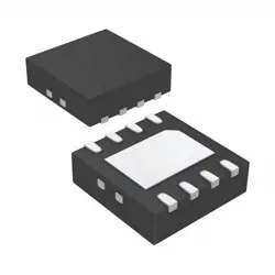
Bilder sind nur zur Referenz
74LVC1G66GW
Analog Switch ICs
- Hersteller
- Fr. Teil #74LVC1G66GW
- Paket
- Datenblatt
- Auf Lager23662
100% Original und Neu
24 Stunden bereit zum Versand
365 Tage Garantie
RFQ & Erhalten Sie mehr Rabatte
Spezifikationen
Übersicht
Description
This IC has two independent switches, which can be controlled by a single enable pin. When activated, it allows the input signal to pass through to the output, while the OFF state isolates the output from the input. The 74LVC1G66GW is designed for efficient power consumption and minimal signal distortion, suitable for applications in telecommunications, consumer electronics, and portable devices.
Its small package size and robust performance make it a popular choice for designers looking to optimize space and efficiency in their circuits. The device is available in various packages, including the SOT-23, making it easy to integrate into different designs.
Features
1. Single Device: It functions as a single analog switch with two inputs and one output.
2. Low Voltage Operation: It operates with a supply voltage range of 1.65V to 5.5V, making it suitable for battery-powered devices.
3. Low On-Resistance: It offers a low on-resistance of typically 0.5Ω at 3.3V, ensuring minimal signal degradation.
4. High Speed: Capable of fast switching speeds, making it ideal for high-frequency applications.
5. Control Logic Levels: Compatible with standard CMOS and TTL logic levels for ease of integration.
6. Power Saving: Low power consumption due to low static current.
7. ESD Protection: Features robust ESD protection to enhance reliability in various environments.
8. Compact Package: Available in a small SOT-23 package, saving PCB space.
These attributes make the 74LVC1G66GW suitable for various applications, including analog signal switching in consumer electronics and communication devices.
Package
Pinout
1. GND (Pin 1): Ground connection.
2. VCCA (Pin 2): Positive power supply voltage input.
3. A (Pin 3): Input terminal for the signal to be switched.
4. Y (Pin 4): Output terminal for the switched signal.
5. S (Pin 5): Control input that determines the switch's on/off state.
When the control input (S) is high, the signal at input A is connected to output Y. When S is low, the connection is open (off). This component is useful in applications where signal routing is required, such as in multiplexing, data switching, or signal isolation.
Manufacturer
Application
Equivalent
1. 74HC1G66
2. 74LVC1G66
3. 74LVC1G66D
4. 74LV1G66
5. TSX1G66
Always verify specifications such as voltage levels, on-resistance, and packaging to ensure compatibility for your specific application.
Versand
VersandmethodenWir
bieten Sie globale Versanddienstleistungen durch DHL, FedEx, TNT, UPS oder einen anderen Spediteur Ihrer Wahl.
Versandgebührenreferenz (DHL/FedEx):
DHL: Versandkosten reichen von $25-$45 (0.5kg), mit einer geschätzten Lieferzeit von 2-5 Werktagen.
von FedEx: Versandkosten reichen von $25-$40 (0.5kg), mit einer geschätzten Lieferzeit von 3-7 Werktagen.
UPS: Versandkosten reichen von $25-$45 (0.5kg), mit einer geschätzten Lieferzeit von 3-7 Werktagen.
TNT: Versandkosten reichen von $25-$65 (0.5kg), mit einer geschätzten Lieferzeit von 3-7 Werktagen.
EMS: Versandkosten reichen von $30-$50 (0.5kg), mit einer geschätzten Lieferzeit von 7-15 Werktagen.
Registrierte Luftpost: Versandkosten sind $ 2- $ 4 (0,1 kg), mit einer geschätzten Lieferzeit von 5-20 Werktagen.
Zahlungen
Payment Methods
Die Zahlungsfrist ist 100% Prepaid.
Derzeit akzeptieren wir nur die folgenden Zahlungsmethoden:
1. PayPal
2. Kredit- / Debitkarte
3. Überweisung
Ähnliche
-
![MX25V1635FZNI]() MX25V1635FZNI
MX25V1635FZNI
Macronix
-
![MX25V1635FZNQ03]() MX25V1635FZNQ03
MX25V1635FZNQ03
Macronix
-
![MX66U1G45GXDI00]() MX66U1G45GXDI00
MX66U1G45GXDI00
Macronix
-
![MX25V4035FZUI]() MX25V4035FZUI
MX25V4035FZUI
Macronix
-
![MX25V16066M2I02]() MX25V16066M2I02
MX25V16066M2I02
Macronix
-
![MX25L8035EM2I-10G]() MX25L8035EM2I-10G
MX25L8035EM2I-10G
Macronix
-
![MX29GL512FHXFI-11G]() MX29GL512FHXFI-11..
MX29GL512FHXFI-11..
Macronix
-
![MX25U51279GXDR00]() MX25U51279GXDR00
MX25U51279GXDR00
Macronix
-
![MX25L6433FM2I-08G]() MX25L6433FM2I-08G
MX25L6433FM2I-08G
Macronix
-
![MX25L12833FM2I-10G]() MX25L12833FM2I-10..
MX25L12833FM2I-10..
Macronix
-
![MX25L12833FZ2I-10G]() MX25L12833FZ2I-10..
MX25L12833FZ2I-10..
Macronix
-
![MX25L12833FZNI-10G]() MX25L12833FZNI-10..
MX25L12833FZNI-10..
Macronix