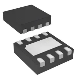
Bilder sind nur zur Referenz
74LVC2G74DP
Flip Flops
- Hersteller
- Fr. Teil #74LVC2G74DP
- Paket
- Datenblatt
- Auf Lager27068
100% Original und Neu
24 Stunden bereit zum Versand
365 Tage Garantie
RFQ & Erhalten Sie mehr Rabatte
Spezifikationen
Übersicht
Description
Each flip-flop in the 74LVC2G74DP features a data (D) input, a clock (CLK) input, and a clear (CLR) input. The flip-flops can store one bit of data and are triggered on the rising edge of the clock signal. The outputs are inverting, providing additional flexibility in circuit design.
This IC is commonly used in applications such as data storage, synchronization, and state machines, where reliable toggling between states is essential. Its small package size and compatibility with various logic levels make it ideal for compact, efficient designs in consumer electronics, automotive, and industrial applications.
Features
1. Dual Flip-Flops: Contains two independent D-type flip-flops.
2. Input Voltage Range: Operates at a wide voltage range from 1.65V to 5.5V, making it suitable for various applications.
3. Low Power Consumption: Designed for low power operation, ideal for battery-powered devices.
4. High-Speed Operation: Capable of high-speed operation with fast propagation delays.
5. 3-State Outputs: Each output can be enabled or disabled, providing flexibility in interfacing with other circuitry.
6. Asynchronous Set and Reset: Allows for direct control of the flip-flops independent of the clock signal.
7. Standard Logic Levels: Compatible with LVC logic levels, ensuring interoperability with other logic families.
8. Small Package: Available in compact packages, suitable for space-constrained applications.
Overall, the 74LVC2G74DP is versatile and efficient, making it ideal for various digital circuit applications.
Package
Pinout
Pin Count and Functions:
1. Pin 1 (D1) - Data input for the first flip-flop.
2. Pin 2 (C1) - Clock input for the first flip-flop.
3. Pin 3 (R1) - Active-low reset input for the first flip-flop.
4. Pin 4 (Q1) - Output for the first flip-flop.
5. Pin 5 (Q1') - Inverted output for the first flip-flop.
6. Pin 6 (D2) - Data input for the second flip-flop.
7. Pin 7 (C2) - Clock input for the second flip-flop.
8. Pin 8 (R2) - Active-low reset input for the second flip-flop.
9. Pin 9 (Q2) - Output for the second flip-flop.
10. Pin 10 (Q2') - Inverted output for the second flip-flop.
The 74LVC2G74DP operates with a supply voltage of 1.65V to 5.5V, providing high-speed operation and low power consumption.
Manufacturer
Application
Equivalent
Versand
VersandmethodenWir
bieten Sie globale Versanddienstleistungen durch DHL, FedEx, TNT, UPS oder einen anderen Spediteur Ihrer Wahl.
Versandgebührenreferenz (DHL/FedEx):
DHL: Versandkosten reichen von $25-$45 (0.5kg), mit einer geschätzten Lieferzeit von 2-5 Werktagen.
von FedEx: Versandkosten reichen von $25-$40 (0.5kg), mit einer geschätzten Lieferzeit von 3-7 Werktagen.
UPS: Versandkosten reichen von $25-$45 (0.5kg), mit einer geschätzten Lieferzeit von 3-7 Werktagen.
TNT: Versandkosten reichen von $25-$65 (0.5kg), mit einer geschätzten Lieferzeit von 3-7 Werktagen.
EMS: Versandkosten reichen von $30-$50 (0.5kg), mit einer geschätzten Lieferzeit von 7-15 Werktagen.
Registrierte Luftpost: Versandkosten sind $ 2- $ 4 (0,1 kg), mit einer geschätzten Lieferzeit von 5-20 Werktagen.
Zahlungen
Payment Methods
Die Zahlungsfrist ist 100% Prepaid.
Derzeit akzeptieren wir nur die folgenden Zahlungsmethoden:
1. PayPal
2. Kredit- / Debitkarte
3. Überweisung
Ähnliche
-
![MX25L3233FM1I-08Q]() MX25L3233FM1I-08Q
MX25L3233FM1I-08Q
Macronix
-
![MX66U1G45GXDI00]() MX66U1G45GXDI00
MX66U1G45GXDI00
Macronix
-
![MX25V5126FM1I]() MX25V5126FM1I
MX25V5126FM1I
Macronix
-
![MX25R3235FZNIL0]() MX25R3235FZNIL0
MX25R3235FZNIL0
Macronix
-
![MX25V16066M2I02]() MX25V16066M2I02
MX25V16066M2I02
Macronix
-
![MX25R6435FBDIL0]() MX25R6435FBDIL0
MX25R6435FBDIL0
Macronix
-
![MX25R1635FZUIH0]() MX25R1635FZUIH0
MX25R1635FZUIH0
Macronix
-
![MX25L6433FM2I-08G]() MX25L6433FM2I-08G
MX25L6433FM2I-08G
Macronix
-
![MX25L12833FZ2I-10G]() MX25L12833FZ2I-10..
MX25L12833FZ2I-10..
Macronix
-
![MX29LV160DTTI-70G]() MX29LV160DTTI-70G
MX29LV160DTTI-70G
Macronix
-
![MX29F040CQI-70G]() MX29F040CQI-70G
MX29F040CQI-70G
Macronix
-
![MX25L25645GXDI-08G]() MX25L25645GXDI-08..
MX25L25645GXDI-08..
Macronix