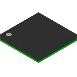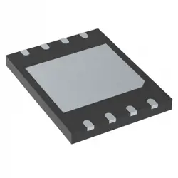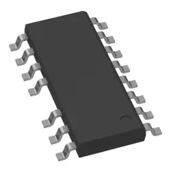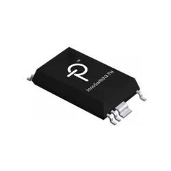
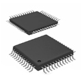
Bilder sind nur zur Referenz
74LVC3G34DC
Buffers & Line Drivers
- Hersteller
- Fr. Teil #74LVC3G34DC
- Paket
- Datenblatt
- Auf Lager16466
100% Original und Neu
24 Stunden bereit zum Versand
365 Tage Garantie
RFQ & Erhalten Sie mehr Rabatte
Spezifikationen
Übersicht
Description
It has a high level of noise immunity and can interface between 1.8V and 5V systems, enhancing flexibility in mixed-voltage designs. The 74LVC3G34DC is available in various package types, making it suitable for space-constrained applications.
Applications include data routing, signal buffering, and as part of more complex digital circuits in consumer electronics, automotive systems, and telecommunications. Its ability to function at low voltage while providing reliable performance makes it a popular choice among engineers for modern electronic designs.
Features
1. Triple Buffer/Driver: Three independent buffers/driver circuits.
2. Low Voltage Operation: Operates with a power supply voltage range of 1.65V to 5.5V, compatible with various logic levels.
3. High Drive Capability: Capable of driving up to 32mA output current, ensuring strong signal integrity.
4. High-Speed Performance: Fast propagation delays, typically around 3.5ns at 3.3V.
5. 3-state Outputs: Each output can be enabled or disabled, allowing for flexible signal routing.
6. Low Static and Dynamic Power Consumption: Reduced power consumption compared to standard logic devices.
7. Wide Operating Temperature Range: Suitable for industrial applications, with a range from -40°C to +125°C.
8. ESD Protection: Designed to withstand electrostatic discharges, enhancing reliability.
These features make the 74LVC3G34DC suitable for a variety of digital applications, including buffers in communication systems and interfacing circuits.
Package
Pinout
1. VCC (Pin 1): Power supply input.
2. GND (Pin 8): Ground reference.
3. A1, A2, A3 (Pins 2, 3, 4): Inputs for the three buffer/driver channels.
4. Y1, Y2, Y3 (Pins 5, 6, 7): Outputs corresponding to the inputs, capable of being in a high-impedance state.
The device operates with a wide supply voltage range (1.65V to 5.5V) and is used in various applications requiring signal buffering, such as interfacing between different logic families or driving capacitive loads. It is designed for low-power consumption and high-speed operation.
Manufacturer
Application
Equivalent
1. 74LVC1G34 - Single buffer/driver.
2. 74LVC2G34 - Dual buffer/driver.
3. 74LVC3G14 - Triple Schmitt-trigger buffer.
4. 74HCT3G34 - High-speed CMOS version for TTL compatibility.
Ensure compatibility with your specific application regarding voltage levels and speed requirements.
Versand
VersandmethodenWir
bieten Sie globale Versanddienstleistungen durch DHL, FedEx, TNT, UPS oder einen anderen Spediteur Ihrer Wahl.
Versandgebührenreferenz (DHL/FedEx):
DHL: Versandkosten reichen von $25-$45 (0.5kg), mit einer geschätzten Lieferzeit von 2-5 Werktagen.
von FedEx: Versandkosten reichen von $25-$40 (0.5kg), mit einer geschätzten Lieferzeit von 3-7 Werktagen.
UPS: Versandkosten reichen von $25-$45 (0.5kg), mit einer geschätzten Lieferzeit von 3-7 Werktagen.
TNT: Versandkosten reichen von $25-$65 (0.5kg), mit einer geschätzten Lieferzeit von 3-7 Werktagen.
EMS: Versandkosten reichen von $30-$50 (0.5kg), mit einer geschätzten Lieferzeit von 7-15 Werktagen.
Registrierte Luftpost: Versandkosten sind $ 2- $ 4 (0,1 kg), mit einer geschätzten Lieferzeit von 5-20 Werktagen.
Zahlungen
Payment Methods
Die Zahlungsfrist ist 100% Prepaid.
Derzeit akzeptieren wir nur die folgenden Zahlungsmethoden:
1. PayPal
2. Kredit- / Debitkarte
3. Überweisung
Ähnliche
-
![MX25V2033FM1I]() MX25V2033FM1I
Macronix
-
![MX25V16066M1I02]() MX25V16066M1I02
Macronix
-
![MX25L25673GMI-10G]() MX25L25673GMI-10G
Macronix
-
![MX29GL512FHXFI-11G]() MX29GL512FHXFI-11..
Macronix
-
![MX25U51279GXDR00]() MX25U51279GXDR00
Macronix
-
![MX25V1635FM2I]() MX25V1635FM2I
Macronix
-
![MX25L6433FM2I-08G]() MX25L6433FM2I-08G
Macronix
-
![MX25L12833FZ2I-10G]() MX25L12833FZ2I-10..
Macronix
-
![MX25L25645GXDI-08G]() MX25L25645GXDI-08..
Macronix
-
![MX25L25735FMI-10G]() MX25L25735FMI-10G
Macronix
-
![MX25L1006EMI-10G]() MX25L1006EMI-10G
Macronix
-
![MX66U1G45GMI00]() MX66U1G45GMI00
Macronix