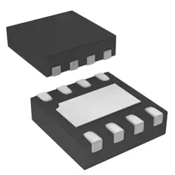
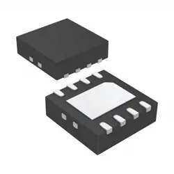
Bilder sind nur zur Referenz
74LVC573APW
Latches 3.3V OCTAL D TRANS LATCH 3-S
- Hersteller
- Fr. Teil #74LVC573APW
- Paket
- Datenblatt
- Auf Lager11466
100% Original und Neu
24 Stunden bereit zum Versand
365 Tage Garantie
RFQ & Erhalten Sie mehr Rabatte
Spezifikationen
| Standard Pack Qty | 75 |
Übersicht
Description
When the latch enable (LE) input is high, data present at the inputs is transferred to the outputs. When LE goes low, the outputs retain the last state, effectively "latching" the data. The 74LVC573APW also includes an active-low output enable (OE) pin for tri-state operation, allowing for easy interfacing with other digital circuits.
It is commonly used in applications where temporary data storage is needed, such as in bus systems, FIFO buffers, and general-purpose data manipulation tasks. The device's low power consumption and fast switching times make it ideal for modern electronic systems. It is available in a TSSOP package, which allows for compact PCB designs.
Features
1. Octal Latch: Contains eight latches that store data.
2. Transparent Mode: Data is transferred to the outputs when the enable (E) input is high.
3. Low-Voltage Operation: Operates from 1.65V to 5.5V, making it suitable for battery-powered devices.
4. High-Speed Performance: Capable of fast switching times, enhancing system speed.
5. 3-State Outputs: Outputs can be placed in a high-impedance state, allowing for bus-oriented applications.
6. Power Consumption: Low static and dynamic power consumption, promoting energy efficiency.
7. Compatible with TTL: Accepts TTL input levels, ensuring compatibility with various logic families.
8. Pin Configuration: Available in a 20-pin TSSOP package, facilitating easy integration into designs.
Overall, the 74LVC573APW is ideal for applications requiring data storage with low power and high-speed performance.
Package
Pinout
### Pin Count and Functions:
1. Pins 1-8: Data inputs (D0-D7)
2. Pin 9: Output enable (OE)
3. Pin 10: Clock input (CLK)
4. Pin 11: Latch enable (LE)
5. Pins 12-19: Data outputs (Q0-Q7)
6. Pin 20: Ground (GND)
### Key Functions:
- D0-D7: Accepts data inputs.
- CLK: Triggers the storage of data into flip-flops.
- LE: Controls whether data is latched (when high, data is stored on the next clock edge).
- OE: Controls the output state (active low).
- Q0-Q7: Provides the stored output data.
This device is typically used in applications requiring temporary data storage and manipulation in digital circuits.
Manufacturer
Application
Equivalent
1. 74LV573
2. 74LVC573
3. 74HC573
4. 74HCT573
Make sure to check specifications like voltage levels and power consumption to ensure compatibility for your application.
Versand
VersandmethodenWir
bieten Sie globale Versanddienstleistungen durch DHL, FedEx, TNT, UPS oder einen anderen Spediteur Ihrer Wahl.
Versandgebührenreferenz (DHL/FedEx):
DHL: Versandkosten reichen von $25-$45 (0.5kg), mit einer geschätzten Lieferzeit von 2-5 Werktagen.
von FedEx: Versandkosten reichen von $25-$40 (0.5kg), mit einer geschätzten Lieferzeit von 3-7 Werktagen.
UPS: Versandkosten reichen von $25-$45 (0.5kg), mit einer geschätzten Lieferzeit von 3-7 Werktagen.
TNT: Versandkosten reichen von $25-$65 (0.5kg), mit einer geschätzten Lieferzeit von 3-7 Werktagen.
EMS: Versandkosten reichen von $30-$50 (0.5kg), mit einer geschätzten Lieferzeit von 7-15 Werktagen.
Registrierte Luftpost: Versandkosten sind $ 2- $ 4 (0,1 kg), mit einer geschätzten Lieferzeit von 5-20 Werktagen.
Zahlungen
Payment Methods
Die Zahlungsfrist ist 100% Prepaid.
Derzeit akzeptieren wir nur die folgenden Zahlungsmethoden:
1. PayPal
2. Kredit- / Debitkarte
3. Überweisung
Ähnliche
-
![MX25L3233FZBI-08Q]() MX25L3233FZBI-08Q
MX25L3233FZBI-08Q
Macronix
-
![MX25V1635FZNI]() MX25V1635FZNI
MX25V1635FZNI
Macronix
-
![MX66U1G45GXDI00]() MX66U1G45GXDI00
MX66U1G45GXDI00
Macronix
-
![MX25V4035FZUI]() MX25V4035FZUI
MX25V4035FZUI
Macronix
-
![MX25V16066M2I02]() MX25V16066M2I02
MX25V16066M2I02
Macronix
-
![MX25L25673GMI-08G]() MX25L25673GMI-08G
MX25L25673GMI-08G
Macronix
-
![MX25L25673GMI-10G]() MX25L25673GMI-10G
MX25L25673GMI-10G
Macronix
-
![MX29GL512FHXFI-11G]() MX29GL512FHXFI-11..
MX29GL512FHXFI-11..
Macronix
-
![MX25V1635FM2I]() MX25V1635FM2I
MX25V1635FM2I
Macronix
-
![MX25U3232FZBI02]() MX25U3232FZBI02
MX25U3232FZBI02
Macronix
-
![MX25L12833FZNI-10G]() MX25L12833FZNI-10..
MX25L12833FZNI-10..
Macronix
-
![MX29LV160DTTI-70G]() MX29LV160DTTI-70G
MX29LV160DTTI-70G
Macronix