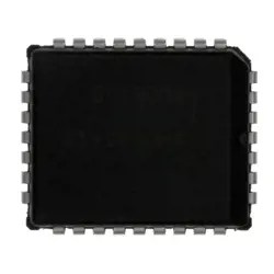
Bilder sind nur zur Referenz
74LVC595APW
Counter Shift Registers 3.3V 8 SHIFT REG OTPT LATCH 3S
- Hersteller
- Fr. Teil #74LVC595APW
- Paket
- Datenblatt
- Auf Lager27385
100% Original und Neu
24 Stunden bereit zum Versand
365 Tage Garantie
RFQ & Erhalten Sie mehr Rabatte
Spezifikationen
| Standard Pack Qty | 96 |
Übersicht
Description
This IC is part of the LVC series, which stands for Low Voltage CMOS, providing low power consumption and high-speed performance. It supports high-speed data transfer rates, making it ideal for interfacing with microcontrollers or digital systems that require expansion of output pins. The 74LVC595APW is often used in applications such as LED displays, data multiplexing, and other digital logic integration tasks. Additionally, it has a tri-state output feature, enabling multiple devices to share the same data bus without conflicts.
Features
1. 8-Bit Storage: It can store 8 bits of data.
2. Serial Input: Data is entered serially, allowing for reduced pin count.
3. Parallel Output: Outputs can be accessed simultaneously, enabling efficient data handling.
4. High-Speed Operation: It operates at a wide range of clock frequencies (up to 100 MHz).
5. Low Power Consumption: Designed for low power operation, making it suitable for battery-powered applications.
6. 3.3V Compatible: It supports 3.3V CMOS logic levels, with a wide input voltage range.
7. Shift Register Functionality: Features a shift register for data manipulation and transfer.
8. Output Enable Control: Allows for control of output states (high impedance) to facilitate device cascading.
9. Temperature Range: Operates across a standard temperature range of -40°C to +125°C.
These features make the 74LVC595APW ideal for various digital applications, such as LED control and data communication interfaces.
Package
Pinout
1. QA to QH (Pins 15-8): Parallel output pins (Q0 to Q7).
2. SRCLR (Pin 1): Shift register clear; active low.
3. SRCK (Pin 2): Shift register clock input; data is shifted on the rising edge.
4. RCLK (Pin 3): Register clock input; transfers the shifted data to the output on the rising edge.
5. SER (Pin 4): Serial data input.
6. OE (Pin 5): Output enable; active low (outputs are enabled when low).
7. VCC (Pin 6): Power supply pin (typically 2.3V to 5.5V).
8. GND (Pin 11): Ground pin.
9. NC (Pins 7, 9, 10): No connect (not used).
The device is commonly used in applications requiring data storage and manipulation, such as LED driving and digital signal processing.
Manufacturer
Application
Equivalent
Versand
VersandmethodenWir
bieten Sie globale Versanddienstleistungen durch DHL, FedEx, TNT, UPS oder einen anderen Spediteur Ihrer Wahl.
Versandgebührenreferenz (DHL/FedEx):
DHL: Versandkosten reichen von $25-$45 (0.5kg), mit einer geschätzten Lieferzeit von 2-5 Werktagen.
von FedEx: Versandkosten reichen von $25-$40 (0.5kg), mit einer geschätzten Lieferzeit von 3-7 Werktagen.
UPS: Versandkosten reichen von $25-$45 (0.5kg), mit einer geschätzten Lieferzeit von 3-7 Werktagen.
TNT: Versandkosten reichen von $25-$65 (0.5kg), mit einer geschätzten Lieferzeit von 3-7 Werktagen.
EMS: Versandkosten reichen von $30-$50 (0.5kg), mit einer geschätzten Lieferzeit von 7-15 Werktagen.
Registrierte Luftpost: Versandkosten sind $ 2- $ 4 (0,1 kg), mit einer geschätzten Lieferzeit von 5-20 Werktagen.
Zahlungen
Payment Methods
Die Zahlungsfrist ist 100% Prepaid.
Derzeit akzeptieren wir nur die folgenden Zahlungsmethoden:
1. PayPal
2. Kredit- / Debitkarte
3. Überweisung
Ähnliche
-
![MX25L3233FZBI-08Q]() MX25L3233FZBI-08Q
MX25L3233FZBI-08Q
Macronix
-
![MX25L3233FM1I-08Q]() MX25L3233FM1I-08Q
MX25L3233FM1I-08Q
Macronix
-
![MX25V5126FM1I]() MX25V5126FM1I
MX25V5126FM1I
Macronix
-
![MX25V2033FM1I]() MX25V2033FM1I
MX25V2033FM1I
Macronix
-
![MX25R6435FBDIL0]() MX25R6435FBDIL0
MX25R6435FBDIL0
Macronix
-
![MX25L25673GMI-08G]() MX25L25673GMI-08G
MX25L25673GMI-08G
Macronix
-
![MX25L25673GMI-10G]() MX25L25673GMI-10G
MX25L25673GMI-10G
Macronix
-
![MX29GL512FHXFI-11G]() MX29GL512FHXFI-11..
MX29GL512FHXFI-11..
Macronix
-
![MX25U51279GXDR00]() MX25U51279GXDR00
MX25U51279GXDR00
Macronix
-
![MX25L12833FM2I-10G]() MX25L12833FM2I-10..
MX25L12833FM2I-10..
Macronix
-
![MX25L12833FZ2I-10G]() MX25L12833FZ2I-10..
MX25L12833FZ2I-10..
Macronix
-
![MX29F040CQI-70G]() MX29F040CQI-70G
MX29F040CQI-70G
Macronix