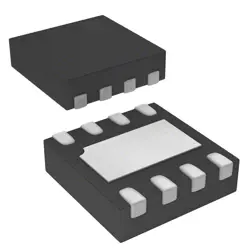
Bilder sind nur zur Referenz
9FGL0451CKILFT
IC CLOCK GENERATOR PCIE 24QFN
- Hersteller
- Fr. Teil #9FGL0451CKILFT
- Paket
- Datenblatt
- Auf Lager4091
100% Original und Neu
24 Stunden bereit zum Versand
365 Tage Garantie
RFQ & Erhalten Sie mehr Rabatte
Spezifikationen
| Part Status | Obsolete |
| DigiKey Programmable | Not Verified |
| PLL | Yes |
| Main Purpose | PCI Express (PCIe) |
| Input | Clock, Crystal |
| Output | HCSL, LVCMOS |
| Number of Circuits | 1 |
| Ratio - Input:Output | 1:2 |
| Differential - Input:Output | No/Yes |
| Frequency - Max | 100MHz |
| Voltage - Supply | 3.135V ~ 3.465V |
| Operating Temperature | -40°C ~ 85°C (TA) |
| Mounting Type | Surface Mount |
| Package / Case | 24-VFQFN Exposed Pad |
| Supplier Device Package | 24-QFN (4x4) |
| Base Product Number | 9FGL0451 |
Übersicht
Description
The designation "9FGL0451CKILFT" likely indicates a particular source located at celestial coordinates or defines its properties, including flux and spectral features. Researchers utilize this catalog to study the nature and distribution of gamma-ray sources, contributing to our understanding of high-energy astrophysics and the underlying processes in the universe.
Features
1. High Data Rate: Supports high-speed data transmission, making it suitable for modern communication systems.
2. Low Power Consumption: Designed for energy efficiency, which is crucial for battery-operated devices.
3. Integrated Functionality: Combines multiple functions within a single chip, reducing the need for additional components.
4. Temperature Range: Operates effectively across a wide temperature range, ensuring reliability in various environments.
5. Compact Size: Features a small form factor, ideal for space-constrained applications.
6. Robust Performance: Offers strong performance in signal integrity and noise immunity.
7. Versatile Applications: Suitable for use in routers, switches, and other networking devices.
This combination of features makes the 9FGL0451CKILFT a versatile choice for next-generation communication systems.
Package
Pinout
1. A0-A14: Address inputs for selecting memory locations.
2. DQ0-DQ7: Data input/output for read and write operations.
3. WE: Write Enable signal to control write operations.
4. RE: Read Enable signal for reading data from the memory.
5. CE: Chip Enable signal to activate the device.
6. Vcc: Power supply pin.
7. GND: Ground pin.
This device is commonly utilized in embedded systems, consumer electronics, and automotive applications due to its robust performance and reliability.
Manufacturer
Application
Equivalent
Versand
VersandmethodenWir
bieten Sie globale Versanddienstleistungen durch DHL, FedEx, TNT, UPS oder einen anderen Spediteur Ihrer Wahl.
Versandgebührenreferenz (DHL/FedEx):
DHL: Versandkosten reichen von $25-$45 (0.5kg), mit einer geschätzten Lieferzeit von 2-5 Werktagen.
von FedEx: Versandkosten reichen von $25-$40 (0.5kg), mit einer geschätzten Lieferzeit von 3-7 Werktagen.
UPS: Versandkosten reichen von $25-$45 (0.5kg), mit einer geschätzten Lieferzeit von 3-7 Werktagen.
TNT: Versandkosten reichen von $25-$65 (0.5kg), mit einer geschätzten Lieferzeit von 3-7 Werktagen.
EMS: Versandkosten reichen von $30-$50 (0.5kg), mit einer geschätzten Lieferzeit von 7-15 Werktagen.
Registrierte Luftpost: Versandkosten sind $ 2- $ 4 (0,1 kg), mit einer geschätzten Lieferzeit von 5-20 Werktagen.
Zahlungen
Payment Methods
Die Zahlungsfrist ist 100% Prepaid.
Derzeit akzeptieren wir nur die folgenden Zahlungsmethoden:
1. PayPal
2. Kredit- / Debitkarte
3. Überweisung
Ähnliche
-
![MX25L3233FZBI-08Q]() MX25L3233FZBI-08Q
MX25L3233FZBI-08Q
Macronix
-
![MX25L3233FM1I-08Q]() MX25L3233FM1I-08Q
MX25L3233FM1I-08Q
Macronix
-
![MX25V1635FZNQ03]() MX25V1635FZNQ03
MX25V1635FZNQ03
Macronix
-
![MX29F400CBTI-70G]() MX29F400CBTI-70G
MX29F400CBTI-70G
Macronix
-
![MX66U1G45GXDI00]() MX66U1G45GXDI00
MX66U1G45GXDI00
Macronix
-
![MX25L8035EM2I-10G]() MX25L8035EM2I-10G
MX25L8035EM2I-10G
Macronix
-
![MX25R6435FBDIL0]() MX25R6435FBDIL0
MX25R6435FBDIL0
Macronix
-
![MX25U25643GZNI00]() MX25U25643GZNI00
MX25U25643GZNI00
Macronix
-
![MX25L2006EM1I-12G]() MX25L2006EM1I-12G
MX25L2006EM1I-12G
Macronix
-
![MX25R1635FZUIH0]() MX25R1635FZUIH0
MX25R1635FZUIH0
Macronix
-
![MX25L6433FM2I-08G]() MX25L6433FM2I-08G
MX25L6433FM2I-08G
Macronix
-
![MX25L12833FM2I-10G]() MX25L12833FM2I-10..
MX25L12833FM2I-10..
Macronix