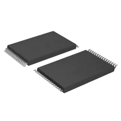
Bilder sind nur zur Referenz
AD8352ACPZ
ADI 0DC Driver
- Hersteller
- Fr. Teil #AD8352ACPZ
- Paket
- Datenblatt
- Auf Lager24605
100% Original und Neu
24 Stunden bereit zum Versand
365 Tage Garantie
RFQ & Erhalten Sie mehr Rabatte
Spezifikationen
| Packaging | Reel |
| Standard Pack Qty | 1500 |
Übersicht
Description
With a low noise figure and high input linearity, the AD8352 provides excellent performance for applications requiring signal integrity. It supports a single-ended input/output configuration, making it easier to integrate into existing systems. The amplifier is powered by a single supply voltage, enhancing its versatility and ease of use.
Key specifications include high dynamic range and fast gain response, making it ideal for automatic gain control (AGC) systems. The AD8352ACPZ is housed in a compact 28-lead LFCSP package, facilitating efficient PCB layout and design. Overall, it is an excellent choice for engineers seeking a robust and flexible VGA solution in RF applications.
Features
1. Wide Frequency Range: Operates from 100 MHz to 3 GHz, suitable for various RF applications.
2. High Gain Control: Offers a gain range of 0 dB to 20 dB with a linear control response.
3. Fast Response Time: Fast gain switching time, enabling quick adjustments for dynamic signals.
4. Low Noise Figure: Achieves a low noise figure, enhancing signal integrity in communication systems.
5. Single Supply Operation: Operates on a single power supply voltage from +3.0 V to +5.5 V.
6. Integrated Control Interface: Features a digital control interface for easy integration into modern systems.
7. High Linearity: Maintains linear performance even at high input levels, reducing distortion.
8. Compact Package: Available in a 32-lead LFCSP package, facilitating PCB space savings.
The AD8352ACPZ is ideal for use in wireless transmitters, receivers, and other RF applications requiring precise gain control.
Package
Pinout
### Pin Functions:
1. RF Input: Pins for receiving the radio frequency input signals.
2. LO Input: Local oscillator input pins for mixing processes.
3. I/Q Inputs: In-phase and quadrature signal inputs for modulation.
4. Output: Differential outputs for the modulated signal.
5. Power Supply (VDD): Connects to the power source, typically +5V.
6. Ground (GND): Common ground connection.
7. Control Pins: Various pins for configuration and operational control (like enabling/disabling functions and gain settings).
The device is suitable for applications such as RF modulation in wireless communications, allowing for compact integration in high-frequency designs.
Manufacturer
Application
Equivalent
Versand
VersandmethodenWir
bieten Sie globale Versanddienstleistungen durch DHL, FedEx, TNT, UPS oder einen anderen Spediteur Ihrer Wahl.
Versandgebührenreferenz (DHL/FedEx):
DHL: Versandkosten reichen von $25-$45 (0.5kg), mit einer geschätzten Lieferzeit von 2-5 Werktagen.
von FedEx: Versandkosten reichen von $25-$40 (0.5kg), mit einer geschätzten Lieferzeit von 3-7 Werktagen.
UPS: Versandkosten reichen von $25-$45 (0.5kg), mit einer geschätzten Lieferzeit von 3-7 Werktagen.
TNT: Versandkosten reichen von $25-$65 (0.5kg), mit einer geschätzten Lieferzeit von 3-7 Werktagen.
EMS: Versandkosten reichen von $30-$50 (0.5kg), mit einer geschätzten Lieferzeit von 7-15 Werktagen.
Registrierte Luftpost: Versandkosten sind $ 2- $ 4 (0,1 kg), mit einer geschätzten Lieferzeit von 5-20 Werktagen.
Zahlungen
Payment Methods
Die Zahlungsfrist ist 100% Prepaid.
Derzeit akzeptieren wir nur die folgenden Zahlungsmethoden:
1. PayPal
2. Kredit- / Debitkarte
3. Überweisung
Ähnliche
-
![MX25R8035FM1IL0]() MX25R8035FM1IL0
MX25R8035FM1IL0
Macronix
-
![MX25L3233FZBI-08Q]() MX25L3233FZBI-08Q
MX25L3233FZBI-08Q
Macronix
-
![MX66U1G45GXDI00]() MX66U1G45GXDI00
MX66U1G45GXDI00
Macronix
-
![MX25V5126FM1I]() MX25V5126FM1I
MX25V5126FM1I
Macronix
-
![MX25V4035FZUI]() MX25V4035FZUI
MX25V4035FZUI
Macronix
-
![MX25V2033FM1I]() MX25V2033FM1I
MX25V2033FM1I
Macronix
-
![MX25V16066M1I02]() MX25V16066M1I02
MX25V16066M1I02
Macronix
-
![MX25L25673GMI-08G]() MX25L25673GMI-08G
MX25L25673GMI-08G
Macronix
-
![MX25U51279GXDR00]() MX25U51279GXDR00
MX25U51279GXDR00
Macronix
-
![MX25U6435FM2I-10G]() MX25U6435FM2I-10G
MX25U6435FM2I-10G
Macronix
-
![MX25L12833FM2I-10G]() MX25L12833FM2I-10..
MX25L12833FM2I-10..
Macronix
-
![MX29F040CTI-70G]() MX29F040CTI-70G
MX29F040CTI-70G
Macronix