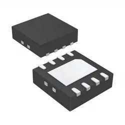
Bilder sind nur zur Referenz
AD8436JCPZ-R7
IC RMS TO DC CONVERTER 20LFCSP
- Hersteller
- Fr. Teil #AD8436JCPZ-R7
- Paket
- Datenblatt
- Auf Lager4452
100% Original und Neu
24 Stunden bereit zum Versand
365 Tage Garantie
RFQ & Erhalten Sie mehr Rabatte
Spezifikationen
| Part Status | Active |
| Current - Supply | 325 µA |
| Voltage - Supply | ±2.4V ~ 18V, 4.8V ~ 36V |
| Mounting Type | Surface Mount |
| Package / Case | 20-WFQFN Exposed Pad, CSP |
| Supplier Device Package | 20-LFCSP (4x4) |
| Base Product Number | AD8436 |
Übersicht
Description
Key specifications include a gain bandwidth product of 120 MHz and a low total harmonic distortion (THD), making it suitable for high-fidelity audio and video applications. The AD8436 operates with a dual power supply, typically ranging from ±2.5 V to ±15 V, and is housed in a compact 8-lead SOIC package, which facilitates easy integration into various circuit designs.
Overall, the AD8436JCPZ-R7 is an excellent choice for applications requiring high precision and speed in differential signal amplification.
Features
1. High Slew Rate: Offers a slew rate of 100 V/µs, enabling fast signal processing.
2. Wide Bandwidth: Gain bandwidth product of 45 MHz, suitable for high-frequency applications.
3. Low Input Offset Voltage: Typically 0.5 mV, ensuring accurate signal amplification.
4. High Open Loop Gain: Approximately 100 dB, providing excellent linearity.
5. Low Noise: Low voltage noise density of 18 nV/√Hz contributes to high fidelity in signal processing.
6. Single-Supply Operation: Can operate from a single supply voltage of 4.5 V to 12 V, simplifying design.
7. Rail-to-Rail Output: Allows output voltage swings close to the supply rails, maximizing dynamic range.
8. Temperature Range: Rated for operation from −40°C to +125°C, suitable for harsh environments.
These features make the AD8436JCPZ-R7 ideal for applications such as data acquisition, sensor signal conditioning, and audio processing.
Package
Pinout
The pin functions are as follows:
1. Pin 1 (V-): Negative supply voltage.
2. Pin 2 (V+): Positive supply voltage.
3. Pins 3, 4, 5, 6 (X1, X2, Y1, Y2): Analog inputs for the two signal multipliers.
4. Pin 7 (Z): Output signal.
5. Pin 8 (GND): Ground.
6. Pins 9 to 16: Various other signal and configuration pins, such as compensation pins and performance enhancement features.
The device is designed for applications requiring high dynamic range and precision, commonly used in signal processing and modulation tasks. For specific configurations and applications, consult the device datasheet for detailed pin descriptions and electrical characteristics.
Manufacturer
Application
Equivalent
Versand
VersandmethodenWir
bieten Sie globale Versanddienstleistungen durch DHL, FedEx, TNT, UPS oder einen anderen Spediteur Ihrer Wahl.
Versandgebührenreferenz (DHL/FedEx):
DHL: Versandkosten reichen von $25-$45 (0.5kg), mit einer geschätzten Lieferzeit von 2-5 Werktagen.
von FedEx: Versandkosten reichen von $25-$40 (0.5kg), mit einer geschätzten Lieferzeit von 3-7 Werktagen.
UPS: Versandkosten reichen von $25-$45 (0.5kg), mit einer geschätzten Lieferzeit von 3-7 Werktagen.
TNT: Versandkosten reichen von $25-$65 (0.5kg), mit einer geschätzten Lieferzeit von 3-7 Werktagen.
EMS: Versandkosten reichen von $30-$50 (0.5kg), mit einer geschätzten Lieferzeit von 7-15 Werktagen.
Registrierte Luftpost: Versandkosten sind $ 2- $ 4 (0,1 kg), mit einer geschätzten Lieferzeit von 5-20 Werktagen.
Zahlungen
Payment Methods
Die Zahlungsfrist ist 100% Prepaid.
Derzeit akzeptieren wir nur die folgenden Zahlungsmethoden:
1. PayPal
2. Kredit- / Debitkarte
3. Überweisung
Ähnliche
-
![MX25L3233FM1I-08Q]() MX25L3233FM1I-08Q
MX25L3233FM1I-08Q
Macronix
-
![MX25V1635FZNQ03]() MX25V1635FZNQ03
MX25V1635FZNQ03
Macronix
-
![MX29F400CBTI-70G]() MX29F400CBTI-70G
MX29F400CBTI-70G
Macronix
-
![MX66U1G45GXDI00]() MX66U1G45GXDI00
MX66U1G45GXDI00
Macronix
-
![MX25R3235FZNIL0]() MX25R3235FZNIL0
MX25R3235FZNIL0
Macronix
-
![MX25V16066M2I02]() MX25V16066M2I02
MX25V16066M2I02
Macronix
-
![MX25L8035EM2I-10G]() MX25L8035EM2I-10G
MX25L8035EM2I-10G
Macronix
-
![MX25L25673GMI-08G]() MX25L25673GMI-08G
MX25L25673GMI-08G
Macronix
-
![MX25L2006EM1I-12G]() MX25L2006EM1I-12G
MX25L2006EM1I-12G
Macronix
-
![MX25L6433FM2I-08G]() MX25L6433FM2I-08G
MX25L6433FM2I-08G
Macronix
-
![MX25L12833FZNI-10G]() MX25L12833FZNI-10..
MX25L12833FZNI-10..
Macronix
-
![MX29F040CQI-70G]() MX29F040CQI-70G
MX29F040CQI-70G
Macronix