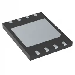
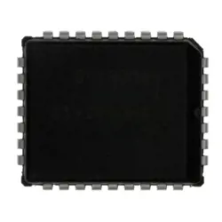
Bilder sind nur zur Referenz
AD8691AKSZ
Precision Amplifiers Single Low Noise CMOS Amplifier
- Hersteller
- Fr. Teil #AD8691AKSZ
- Paket
- Datenblatt AD8691AKSZ DataSheet
- Auf Lager27892
100% Original und Neu
24 Stunden bereit zum Versand
365 Tage Garantie
RFQ & Erhalten Sie mehr Rabatte
Spezifikationen
| Standard Pack Qty | 3000 |
| Packaging | Reel |
Übersicht
Description
Key specifications include a wide supply voltage range of 2.7V to 36V, high gain bandwidth product, and low distortion, making it suitable for both DC and AC signal processing. The device operates with low power consumption, making it a good choice for battery-powered applications.
Its small package size (e.g., MSOP or LFCSP) supports compact designs. The AD8691AKSZ is renowned for its stability and reliability in various environments, ensuring consistent performance across temperature variations. Overall, it is an excellent choice for engineers seeking a robust operational amplifier for precision applications.
Features
1. Low Offset Voltage: Typically 50 µV, ensuring high accuracy in signal processing.
2. Low Noise: Voltage noise density of 8 nV/√Hz at 1 kHz, minimizing interference in sensitive applications.
3. Rail-to-Rail Output: Allows the output to swing from rail to rail, maximizing output range.
4. Wide Supply Voltage Range: Operates from 2.7 V to 36 V, suitable for battery-powered and high-voltage systems.
5. High Gain Bandwidth Product: 1 MHz, enabling good performance in a variety of feedback configurations.
6. Low Power Consumption: With a quiescent current of 75 µA per amplifier, it is energy-efficient for portable applications.
7. Single and Dual Supply Operation: Versatile for different circuit designs.
8. Temperature Range: Operates over a wide temperature range (-40°C to +125°C).
These features make the AD8691AKSZ ideal for precision measurement applications, medical devices, and industrial instrumentation.
Package
Pinout
The pin functions are as follows:
1. Inverting Input (–): Pin 1, where the input signal for inversion is applied.
2. Non-inverting Input (+): Pin 2, where the input signal for amplification is applied.
3. Output: Pin 3, where the amplified signal is output.
4. Negative Supply (V–): Pin 4, connected to the negative supply voltage.
5. Positive Supply (V+): Pin 5, connected to the positive supply voltage.
6. NC (No Connect): Pin 6, not internally connected to the device.
7. NC (No Connect): Pin 7, not internally connected to the device.
8. Compensation (Comp): Pin 8, used for frequency compensation in certain configurations.
The AD8691 features low offset voltage, low noise, and high precision, making it suitable for precision applications.
Manufacturer
Application
Equivalent
Versand
VersandmethodenWir
bieten Sie globale Versanddienstleistungen durch DHL, FedEx, TNT, UPS oder einen anderen Spediteur Ihrer Wahl.
Versandgebührenreferenz (DHL/FedEx):
DHL: Versandkosten reichen von $25-$45 (0.5kg), mit einer geschätzten Lieferzeit von 2-5 Werktagen.
von FedEx: Versandkosten reichen von $25-$40 (0.5kg), mit einer geschätzten Lieferzeit von 3-7 Werktagen.
UPS: Versandkosten reichen von $25-$45 (0.5kg), mit einer geschätzten Lieferzeit von 3-7 Werktagen.
TNT: Versandkosten reichen von $25-$65 (0.5kg), mit einer geschätzten Lieferzeit von 3-7 Werktagen.
EMS: Versandkosten reichen von $30-$50 (0.5kg), mit einer geschätzten Lieferzeit von 7-15 Werktagen.
Registrierte Luftpost: Versandkosten sind $ 2- $ 4 (0,1 kg), mit einer geschätzten Lieferzeit von 5-20 Werktagen.
Zahlungen
Payment Methods
Die Zahlungsfrist ist 100% Prepaid.
Derzeit akzeptieren wir nur die folgenden Zahlungsmethoden:
1. PayPal
2. Kredit- / Debitkarte
3. Überweisung
Ähnliche
-
![MX25L3233FZBI-08Q]() MX25L3233FZBI-08Q
Macronix
-
![MX25V1635FZNI]() MX25V1635FZNI
Macronix
-
![MX66U1G45GXDI00]() MX66U1G45GXDI00
Macronix
-
![MX25V16066M1I02]() MX25V16066M1I02
Macronix
-
![MX25V16066M2I02]() MX25V16066M2I02
Macronix
-
![MX25L25673GMI-10G]() MX25L25673GMI-10G
Macronix
-
![MX25U25643GZNI00]() MX25U25643GZNI00
Macronix
-
![MX25L6433FM2I-08G]() MX25L6433FM2I-08G
Macronix
-
![MX25L12833FM2I-10G]() MX25L12833FM2I-10..
Macronix
-
![MX25L12833FZ2I-10G]() MX25L12833FZ2I-10..
Macronix
-
![MX25L12835FZ2I-10G]() MX25L12835FZ2I-10..
Macronix
-
![MX29F040CQI-70G]() MX29F040CQI-70G
Macronix