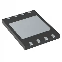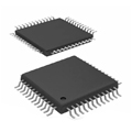
Bilder sind nur zur Referenz
ADCLK905BCPZ
ADI 1:1 ECL, 7 Gbpps CLOCK/DATA BUFFERS
- Hersteller
- Fr. Teil #ADCLK905BCPZ
- Paket
- Datenblatt
- Auf Lager16345
100% Original und Neu
24 Stunden bereit zum Versand
365 Tage Garantie
RFQ & Erhalten Sie mehr Rabatte
Spezifikationen
| Standard Pack Qty | 50 |
Übersicht
Description
The device typically supports LVPECL and LVDS output formats, ensuring compatibility with a range of high-speed logic families. Its ability to drive multiple loads while maintaining signal integrity makes it suitable for communication systems, data converters, and networking equipment.
With a power supply range of 3.0V to 3.6V, the ADCLK905BCPZ also boasts low power consumption, making it efficient for power-sensitive applications. Additionally, it includes functionalities like enable/disable control, enhancing its versatility in various circuit configurations. Overall, the ADCLK905BCPZ is an essential component for engineers looking to improve the performance of timing signals in complex electronic systems.
Features
1. Low Jitter Performance: It offers low phase noise and jitter, making it suitable for high-speed data applications.
2. Wide Operating Frequency Range: Supports clock frequencies up to 1.5 GHz, accommodating various system requirements.
3. Multiple Outputs: Provides multiple low-skew outputs, ensuring synchronized clock signals across different components.
4. Integrated Voltage Level Shifting: Allows compatibility with various logic levels, enhancing design flexibility.
5. Power Supply Range: Operates from a single 3.3V power supply, simplifying power management.
6. Compact Package: Available in a 32-lead LFCSP package, enabling space-efficient designs.
7. Low Power Consumption: Designed for energy-efficient operation, suitable for portable applications.
These features make the ADCLK905BCPZ ideal for use in telecommunications, data communications, and high-speed digital systems.
Package
Pinout
The primary functions of the ADCLK905BCPZ include:
1. Clock Buffering: It provides multiple buffered outputs from a single input clock signal, which helps in driving high-capacitance loads.
2. Low Jitter Performance: The device is designed for low additive jitter, making it suitable for high-performance applications.
3. Output Control: The chip includes features for controlling the output enable/disable function.
4. Voltage Supply: It operates over a wide supply voltage range, typically from 2.5V to 3.3V.
The 16 pins serve various functions including power supply, ground, input clock, multiple output clocks, and control signals. For precise applications, refer to the specific datasheet for detailed pin assignments and functionalities.
Manufacturer
Application
Equivalent
Versand
VersandmethodenWir
bieten Sie globale Versanddienstleistungen durch DHL, FedEx, TNT, UPS oder einen anderen Spediteur Ihrer Wahl.
Versandgebührenreferenz (DHL/FedEx):
DHL: Versandkosten reichen von $25-$45 (0.5kg), mit einer geschätzten Lieferzeit von 2-5 Werktagen.
von FedEx: Versandkosten reichen von $25-$40 (0.5kg), mit einer geschätzten Lieferzeit von 3-7 Werktagen.
UPS: Versandkosten reichen von $25-$45 (0.5kg), mit einer geschätzten Lieferzeit von 3-7 Werktagen.
TNT: Versandkosten reichen von $25-$65 (0.5kg), mit einer geschätzten Lieferzeit von 3-7 Werktagen.
EMS: Versandkosten reichen von $30-$50 (0.5kg), mit einer geschätzten Lieferzeit von 7-15 Werktagen.
Registrierte Luftpost: Versandkosten sind $ 2- $ 4 (0,1 kg), mit einer geschätzten Lieferzeit von 5-20 Werktagen.
Zahlungen
Payment Methods
Die Zahlungsfrist ist 100% Prepaid.
Derzeit akzeptieren wir nur die folgenden Zahlungsmethoden:
1. PayPal
2. Kredit- / Debitkarte
3. Überweisung
Ähnliche
-
![MX25L3233FZBI-08Q]() MX25L3233FZBI-08Q
Macronix
-
![MX29F400CBTI-70G]() MX29F400CBTI-70G
Macronix
-
![MX25V5126FM1I]() MX25V5126FM1I
Macronix
-
![MX25V4035FZUI]() MX25V4035FZUI
Macronix
-
![MX25R6435FBDIL0]() MX25R6435FBDIL0
Macronix
-
![MX25U51279GXDR00]() MX25U51279GXDR00
Macronix
-
![MX25U25643GZNI00]() MX25U25643GZNI00
Macronix
-
![MX25L6433FM2I-08G]() MX25L6433FM2I-08G
Macronix
-
![MX25L12835FZ2I-10G]() MX25L12835FZ2I-10..
Macronix
-
![MX29LV160DTTI-70G]() MX29LV160DTTI-70G
Macronix
-
![MX29F040CTI-70G]() MX29F040CTI-70G
Macronix
-
![MX66U1G45GMI00]() MX66U1G45GMI00
Macronix