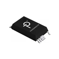
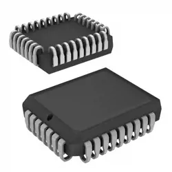
Bilder sind nur zur Referenz
ADL5530ACPZ
- Hersteller
- Fr. Teil #ADL5530ACPZ
- Paket
- Datenblatt
- Auf Lager2870
100% Original und Neu
24 Stunden bereit zum Versand
365 Tage Garantie
RFQ & Erhalten Sie mehr Rabatte
Spezifikationen
| Brand | Analog Devices |
| Factory Pack Quantity:Factory Pack Quantity | 3000 |
Übersicht
Description
Key attributes include a supply voltage range of 4.5 V to 5.5 V and low power consumption, which enhances its suitability for portable applications. The ADL5530ACPZ utilizes a compact package design, facilitating easy integration into various systems. Additionally, it offers features like adjustable gain, enabling flexibility in diverse applications.
Overall, the ADL5530ACPZ is a versatile component that addresses the needs of modern RF signal processing, providing robust performance in a compact form factor.
Features
1. Wide Bandwidth: Operates effectively from DC to 1.0 GHz, making it suitable for RF and baseband applications.
2. Gain Control: Offers a programmable gain range of 0 to 31.5 dB with a 0.5 dB step size, allowing for fine adjustment.
3. Low Noise: Features a low noise figure (NF) of 1.2 dB at maximum gain, enhancing the signal-to-noise ratio.
4. High Linearity: Exhibits excellent linearity, making it ideal for applications that handle complex signals.
5. Single Supply Operation: Requires only a single supply voltage of 5V, simplifying design and integration.
6. Integrated Features: Includes a shutdown mode for power savings, and a low distortion characteristic for high-fidelity signal processing.
7. Temperature Range: Qualified for operation from -40°C to +85°C, suitable for industrial applications.
These features make the ADL5530ACPZ a versatile choice for communications, instrumentation, and imaging systems.
Package
Pinout
Key pins and their functions include:
1. RF Input (Pin 1 & Pin 2): For receiving RF signals.
2. RF Output (Pin 3): For outputting the amplified RF signal.
3. VDD (Pin 4 & Pin 5): Supply voltage inputs for powering the device.
4. GND (Pin 6 & Pin 7): Ground connections to provide a reference point.
5. Control Pins (like Pin 9 & Pin 10): Used for gain control and other adjustments.
6. Bypass Capacitor Pins (Pin 8, Pin 11): For stability and noise reduction.
7. NC (No Connect Pins, e.g., Pin 12): Not connected internally.
This amplifier is designed to operate over a wide frequency range, making it versatile for various RF applications.
Manufacturer
Application
Equivalent
Versand
VersandmethodenWir
bieten Sie globale Versanddienstleistungen durch DHL, FedEx, TNT, UPS oder einen anderen Spediteur Ihrer Wahl.
Versandgebührenreferenz (DHL/FedEx):
DHL: Versandkosten reichen von $25-$45 (0.5kg), mit einer geschätzten Lieferzeit von 2-5 Werktagen.
von FedEx: Versandkosten reichen von $25-$40 (0.5kg), mit einer geschätzten Lieferzeit von 3-7 Werktagen.
UPS: Versandkosten reichen von $25-$45 (0.5kg), mit einer geschätzten Lieferzeit von 3-7 Werktagen.
TNT: Versandkosten reichen von $25-$65 (0.5kg), mit einer geschätzten Lieferzeit von 3-7 Werktagen.
EMS: Versandkosten reichen von $30-$50 (0.5kg), mit einer geschätzten Lieferzeit von 7-15 Werktagen.
Registrierte Luftpost: Versandkosten sind $ 2- $ 4 (0,1 kg), mit einer geschätzten Lieferzeit von 5-20 Werktagen.
Zahlungen
Payment Methods
Die Zahlungsfrist ist 100% Prepaid.
Derzeit akzeptieren wir nur die folgenden Zahlungsmethoden:
1. PayPal
2. Kredit- / Debitkarte
3. Überweisung
Ähnliche
-
![MX25L3233FZBI-08Q]() MX25L3233FZBI-08Q
MX25L3233FZBI-08Q
Macronix
-
![MX66U1G45GXDI00]() MX66U1G45GXDI00
MX66U1G45GXDI00
Macronix
-
![MX25V5126FM1I]() MX25V5126FM1I
MX25V5126FM1I
Macronix
-
![MX25U25643GZNI00]() MX25U25643GZNI00
MX25U25643GZNI00
Macronix
-
![MX25U6435FM2I-10G]() MX25U6435FM2I-10G
MX25U6435FM2I-10G
Macronix
-
![MX29LV640ETTI-70G]() MX29LV640ETTI-70G
MX29LV640ETTI-70G
Macronix
-
![MX25L1006EMI-10G]() MX25L1006EMI-10G
MX25L1006EMI-10G
Macronix
-
![MX66U1G45GMI00]() MX66U1G45GMI00
MX66U1G45GMI00
Macronix
-
![MX25L4006EM2I-12G]() MX25L4006EM2I-12G
MX25L4006EM2I-12G
Macronix
-
![MX25R4035FM1IL0]() MX25R4035FM1IL0
MX25R4035FM1IL0
Macronix
-
![MX25L6473FM2I-08G]() MX25L6473FM2I-08G
MX25L6473FM2I-08G
Macronix
-
![MX29LV040CQI-70G]() MX29LV040CQI-70G
MX29LV040CQI-70G
Macronix