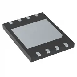
Bilder sind nur zur Referenz
ADL5610ARKZ
ADI 2dB Noise Figure Gain Block
- Hersteller
- Fr. Teil #ADL5610ARKZ
- Paket
- Datenblatt
- Auf Lager5749
100% Original und Neu
24 Stunden bereit zum Versand
365 Tage Garantie
RFQ & Erhalten Sie mehr Rabatte
Spezifikationen
| Standard Pack Qty | 1000 |
Übersicht
Description
Key features of the ADL5610ARKZ include a high gain of up to 20 dB, low noise figure, and excellent linearity, which contribute to improved signal integrity and overall system performance. The amplifier provides a programmable gain control (PGC) option, allowing for versatile operation across different signal conditions.
Its compact package and low power consumption make it ideal for integration into portable devices and systems. The ADL5610ARKZ is also noted for its thermal stability and reliability, ensuring consistent performance in diverse environmental conditions.
Overall, the ADL5610ARKZ is a vital component for engineers seeking to enhance the efficiency and effectiveness of RF signal amplification in modern communication technologies.
Features
1. Frequency Range: Operates from 0.1 GHz to 6.0 GHz, making it suitable for multiple RF bands.
2. Gain: Provides a high gain of up to 20 dB, ensuring strong amplification of weak signals.
3. High Linearity: Exhibits excellent linearity, enabling clean signal amplification and minimizing distortion.
4. Low Noise Figure: Features a low noise figure (NF), typically around 2.2 dB, enhancing signal-to-noise ratio (SNR).
5. Supply Voltage: Operates on a supply voltage range of 4.5 V to 5.5 V, allowing for flexibility in power supply designs.
6. Temperature Range: Designed to operate in a wide temperature range, from -40°C to +85°C, ensuring reliability in various environments.
7. Package Type: Offered in a compact, lead-free LFCSP package for minimized PCB space.
Overall, the ADL5610ARKZ is ideal for applications requiring robust performance in RF signal amplification.
Package
Pinout
The primary functions of the pins include:
1. Power Supply Pins: Provide operating voltage (VDD) to the amplifier.
2. Signal Input Pins: Accept RF input signals (RFIN1, RFIN2) for the two channels.
3. Signal Output Pins: Deliver amplified RF output signals (RFOUT1, RFOUT2).
4. Biasing Pins: Control the biasing of the amplifier for optimal performance.
5. Ground Pins: Provide a common ground reference (GND).
6. Control Pins: Enable or disable the amplifier functions, adjusting gain settings as needed.
For specific pin assignments and detailed electrical characteristics, refer to the ADL5610 datasheet.
Manufacturer
Application
Equivalent
Versand
VersandmethodenWir
bieten Sie globale Versanddienstleistungen durch DHL, FedEx, TNT, UPS oder einen anderen Spediteur Ihrer Wahl.
Versandgebührenreferenz (DHL/FedEx):
DHL: Versandkosten reichen von $25-$45 (0.5kg), mit einer geschätzten Lieferzeit von 2-5 Werktagen.
von FedEx: Versandkosten reichen von $25-$40 (0.5kg), mit einer geschätzten Lieferzeit von 3-7 Werktagen.
UPS: Versandkosten reichen von $25-$45 (0.5kg), mit einer geschätzten Lieferzeit von 3-7 Werktagen.
TNT: Versandkosten reichen von $25-$65 (0.5kg), mit einer geschätzten Lieferzeit von 3-7 Werktagen.
EMS: Versandkosten reichen von $30-$50 (0.5kg), mit einer geschätzten Lieferzeit von 7-15 Werktagen.
Registrierte Luftpost: Versandkosten sind $ 2- $ 4 (0,1 kg), mit einer geschätzten Lieferzeit von 5-20 Werktagen.
Zahlungen
Payment Methods
Die Zahlungsfrist ist 100% Prepaid.
Derzeit akzeptieren wir nur die folgenden Zahlungsmethoden:
1. PayPal
2. Kredit- / Debitkarte
3. Überweisung
Ähnliche
-
![MX29F400CBTI-70G]() MX29F400CBTI-70G
Macronix
-
![MX25V4035FZUI]() MX25V4035FZUI
Macronix
-
![MX25V16066M2I02]() MX25V16066M2I02
Macronix
-
![MX25R6435FBDIL0]() MX25R6435FBDIL0
Macronix
-
![MX25L25673GMI-08G]() MX25L25673GMI-08G
Macronix
-
![MX25L25673GMI-10G]() MX25L25673GMI-10G
Macronix
-
![MX25U51279GXDR00]() MX25U51279GXDR00
Macronix
-
![MX25L2006EM1I-12G]() MX25L2006EM1I-12G
Macronix
-
![MX25L6433FM2I-08G]() MX25L6433FM2I-08G
Macronix
-
![MX25L12833FZ2I-10G]() MX25L12833FZ2I-10..
Macronix
-
![MX25U25645GXDI00]() MX25U25645GXDI00
Macronix
-
![MX25L25645GXDI-08G]() MX25L25645GXDI-08..
Macronix