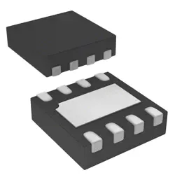
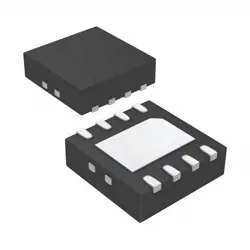
Bilder sind nur zur Referenz
CXDQ3BFAM-CQ-A
- Hersteller
- Fr. Teil #CXDQ3BFAM-CQ-A
- Paket
- Datenblatt CXDQ3BFAM-CQ-A DataSheet
- Auf Lager20276
100% Original und Neu
24 Stunden bereit zum Versand
365 Tage Garantie
RFQ & Erhalten Sie mehr Rabatte
Spezifikationen
| Manufacturer | CXMT |
| Package | BGA-96(13x7.5) |
| Memory Size | 8Gbit |
| Operating Temperature | 0℃~+95℃ |
| Memory Format | SDRAM DDR4 |
| Voltage - Supply | 1.14V~1.26V |
| Current - Supply | 105.8mA |
Übersicht
Description
If the context involves a specific industry, product specifications, or a particular technology, it would be essential to look into relevant documentation or resources for detailed information. For a comprehensive understanding, including features, applications, and specifications, consulting the manufacturer's guidelines or technical sheets would be advisable. If you have additional context or specific questions regarding CXDQ3BFAM-CQ-A, please provide that for a more tailored response.
Features
1. Efficiency: Offers high energy efficiency, minimizing heat loss and extending the lifespan of connected LEDs.
2. Dimming Capability: Supports multiple dimming methods, allowing for versatile control over light intensity.
3. Wide Input Voltage Range: Accommodates a broad range of input voltages, ensuring compatibility with different power sources.
4. Compact Design: Its small form factor makes it suitable for space-constrained environments.
5. Thermal Protection: Equipped with thermal protection features to prevent overheating, enhancing reliability.
6. Robust Output: Provides stable and consistent output current, ensuring optimal performance of LED lights.
7. Ease of Integration: Designed for straightforward installation and integration into a variety of lighting systems.
Overall, the CXDQ3BFAM-CQ-A is ideal for applications requiring efficient and reliable LED driving solutions.
Package
Pinout
The primary functions of the pins include:
1. Power Supply: VCC (power) and GND (ground) pins for powering the device.
2. Data Lines: Four data input/output pins (D0, D1, D2, D3) for quad data communication.
3. Control Pins:
- SCLK: Serial clock input for timing data transfer.
- CS#: Chip select, used to enable communication with the device.
- WP#: Write protect, to prevent accidental data modification.
- HOLD#: Hold pin, to pause the operation without losing data.
These pins facilitate high-speed data transfer and control functionality, making it suitable for embedded applications. Always refer to the specific datasheet for precise details and pin assignments.
Manufacturer
Application
Equivalent
Versand
VersandmethodenWir
bieten Sie globale Versanddienstleistungen durch DHL, FedEx, TNT, UPS oder einen anderen Spediteur Ihrer Wahl.
Versandgebührenreferenz (DHL/FedEx):
DHL: Versandkosten reichen von $25-$45 (0.5kg), mit einer geschätzten Lieferzeit von 2-5 Werktagen.
von FedEx: Versandkosten reichen von $25-$40 (0.5kg), mit einer geschätzten Lieferzeit von 3-7 Werktagen.
UPS: Versandkosten reichen von $25-$45 (0.5kg), mit einer geschätzten Lieferzeit von 3-7 Werktagen.
TNT: Versandkosten reichen von $25-$65 (0.5kg), mit einer geschätzten Lieferzeit von 3-7 Werktagen.
EMS: Versandkosten reichen von $30-$50 (0.5kg), mit einer geschätzten Lieferzeit von 7-15 Werktagen.
Registrierte Luftpost: Versandkosten sind $ 2- $ 4 (0,1 kg), mit einer geschätzten Lieferzeit von 5-20 Werktagen.
Zahlungen
Payment Methods
Die Zahlungsfrist ist 100% Prepaid.
Derzeit akzeptieren wir nur die folgenden Zahlungsmethoden:
1. PayPal
2. Kredit- / Debitkarte
3. Überweisung
Ähnliche
-
![MX25L3233FZBI-08Q]() MX25L3233FZBI-08Q
MX25L3233FZBI-08Q
Macronix
-
![MX25V1635FZNI]() MX25V1635FZNI
MX25V1635FZNI
Macronix
-
![MX29F400CBTI-70G]() MX29F400CBTI-70G
MX29F400CBTI-70G
Macronix
-
![MX25V16066M1I02]() MX25V16066M1I02
MX25V16066M1I02
Macronix
-
![MX25V16066M2I02]() MX25V16066M2I02
MX25V16066M2I02
Macronix
-
![MX29GL512FHXFI-11G]() MX29GL512FHXFI-11..
MX29GL512FHXFI-11..
Macronix
-
![MX25U25643GZNI00]() MX25U25643GZNI00
MX25U25643GZNI00
Macronix
-
![MX25L2006EM1I-12G]() MX25L2006EM1I-12G
MX25L2006EM1I-12G
Macronix
-
![MX25R1635FZUIH0]() MX25R1635FZUIH0
MX25R1635FZUIH0
Macronix
-
![MX25L12833FM2I-10G]() MX25L12833FM2I-10..
MX25L12833FM2I-10..
Macronix
-
![MX25L12833FZNI-10G]() MX25L12833FZNI-10..
MX25L12833FZNI-10..
Macronix
-
![MX25L12835FZ2I-10G]() MX25L12835FZ2I-10..
MX25L12835FZ2I-10..
Macronix