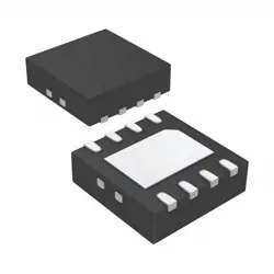
Bilder sind nur zur Referenz
CY14B101LA-SP45XI
IC NVSRAM 1MBIT PARALLEL 48SSOP
- Hersteller
- Fr. Teil #CY14B101LA-SP45XI
- Paket
- Datenblatt CY14B101LA-SP45XI DataSheet
- Auf Lager9581
100% Original und Neu
24 Stunden bereit zum Versand
365 Tage Garantie
RFQ & Erhalten Sie mehr Rabatte
Spezifikationen
| Part Status | Active |
| DigiKey Programmable | Not Verified |
| Memory Type | Non-Volatile |
| Memory Format | NVSRAM |
| Technology | NVSRAM (Non-Volatile SRAM) |
| Memory Size | 1Mbit |
| Memory Organization | 128K x 8 |
| Memory Interface | Parallel |
| Write Cycle Time - Word, Page | 45ns |
| Voltage - Supply | 2.7V ~ 3.6V |
| Operating Temperature | -40°C ~ 85°C (TA) |
| Mounting Type | Surface Mount |
| Package / Case | 48-BSSOP (0.295", 7.50mm Width) |
| Supplier Device Package | 48-SSOP |
| Base Product Number | CY14B101 |
| Access Time | 45 ns |
Übersicht
Description
Features
1. Interface: It uses a Serial Peripheral Interface (SPI) for fast data transfers.
2. High Speed: The device supports clock rates up to 45 MHz, enabling quick access times.
3. Endurance: Offers up to 1 million write/erase cycles, ensuring durability for applications requiring frequent updates.
4. Data Retention: Retains data for over 100 years, making it suitable for long-term storage applications.
5. Low Power Consumption: Operates at low voltage (2.7V to 3.6V) and consumes minimal power in standby and active modes.
6. Package Options: Available in various packages, including SOIC and TSSOP, facilitating integration into different designs.
7. Security Features: Includes write protection and locking capabilities to secure stored data.
This combination of features makes the CY14B101LA-SP45XI ideal for applications in industrial, automotive, and consumer electronics.
Package
Pinout
Pin Functions:
1. Address Pins (A0-A16): Used to select memory locations.
2. Data Pins (D0-D7): Bi-directional data bus for read and write operations.
3. Chip Enable (CE): Activates the device for read/write operations.
4. Write Enable (WE): Controls write operations; active low.
5. Output Enable (OE): Controls the output drivers; active low.
6. VCC: Power supply pin.
7. VSS: Ground reference.
8. WP (Write Protect): Used to enable or disable write operations.
This device combines SRAM speed with non-volatility, making it suitable for applications requiring fast access and data retention without power.
Manufacturer
Application
Equivalent
1. Microchip SST26VF010B
2. Winbond W25Q16JV
3. Adesto AT25DF041A
4. GigaDevice GD25Q16C
Always verify compatibility based on specific application requirements such as voltage, speed, and packaging.
Versand
VersandmethodenWir
bieten Sie globale Versanddienstleistungen durch DHL, FedEx, TNT, UPS oder einen anderen Spediteur Ihrer Wahl.
Versandgebührenreferenz (DHL/FedEx):
DHL: Versandkosten reichen von $25-$45 (0.5kg), mit einer geschätzten Lieferzeit von 2-5 Werktagen.
von FedEx: Versandkosten reichen von $25-$40 (0.5kg), mit einer geschätzten Lieferzeit von 3-7 Werktagen.
UPS: Versandkosten reichen von $25-$45 (0.5kg), mit einer geschätzten Lieferzeit von 3-7 Werktagen.
TNT: Versandkosten reichen von $25-$65 (0.5kg), mit einer geschätzten Lieferzeit von 3-7 Werktagen.
EMS: Versandkosten reichen von $30-$50 (0.5kg), mit einer geschätzten Lieferzeit von 7-15 Werktagen.
Registrierte Luftpost: Versandkosten sind $ 2- $ 4 (0,1 kg), mit einer geschätzten Lieferzeit von 5-20 Werktagen.
Zahlungen
Payment Methods
Die Zahlungsfrist ist 100% Prepaid.
Derzeit akzeptieren wir nur die folgenden Zahlungsmethoden:
1. PayPal
2. Kredit- / Debitkarte
3. Überweisung
Ähnliche
-
![MX25R8035FM1IL0]() MX25R8035FM1IL0
MX25R8035FM1IL0
Macronix
-
![MX25L3233FZBI-08Q]() MX25L3233FZBI-08Q
MX25L3233FZBI-08Q
Macronix
-
![MX25L3233FM1I-08Q]() MX25L3233FM1I-08Q
MX25L3233FM1I-08Q
Macronix
-
![MX25V1635FZNI]() MX25V1635FZNI
MX25V1635FZNI
Macronix
-
![MX66U1G45GXDI00]() MX66U1G45GXDI00
MX66U1G45GXDI00
Macronix
-
![MX25V5126FM1I]() MX25V5126FM1I
MX25V5126FM1I
Macronix
-
![MX25V4035FZUI]() MX25V4035FZUI
MX25V4035FZUI
Macronix
-
![MX25V16066M1I02]() MX25V16066M1I02
MX25V16066M1I02
Macronix
-
![MX25L25673GMI-08G]() MX25L25673GMI-08G
MX25L25673GMI-08G
Macronix
-
![MX25U25643GZNI00]() MX25U25643GZNI00
MX25U25643GZNI00
Macronix
-
![MX25L12833FM2I-10G]() MX25L12833FM2I-10..
MX25L12833FM2I-10..
Macronix
-
![MX25L12833FZNI-10G]() MX25L12833FZNI-10..
MX25L12833FZNI-10..
Macronix