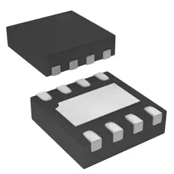
Bilder sind nur zur Referenz
CY2890-F02
- Hersteller
- Fr. Teil #CY2890-F02
- Paket
- Datenblatt
- Auf Lager9058
100% Original und Neu
24 Stunden bereit zum Versand
365 Tage Garantie
RFQ & Erhalten Sie mehr Rabatte
Spezifikationen
| Manufacturer | JLCPCB Assembly |
| Package | LQFP-64_L7.0-W7.0-P0.40-LS9.0-BL |
Übersicht
Description
Key features include programmable output frequencies, low power consumption, and flexibility in configuration, allowing it to cater to different system requirements. It supports various interfaces for easy integration with microcontrollers and other digital systems. The CY2890-F02 is often used in applications such as networking equipment, high-speed computing, and consumer electronics, where accurate timing is crucial for optimal performance. Overall, it provides a reliable solution for designers looking to implement robust timing circuits in their products.
Features
1. Frequency Range: It supports a wide frequency range, typically from 1 MHz to several hundred MHz, allowing it to generate various clock frequencies.
2. Low Jitter: The device offers low phase noise and jitter performance, making it ideal for high-speed data communication systems.
3. Multiple Output Clocks: It can provide multiple clock outputs, allowing for synchronization across different components within a system.
4. Programmability: The CY2890-F02 is programmable via I2C or SPI interfaces, enabling easy configuration and integration into custom applications.
5. Power Efficiency: Designed for low power consumption, it helps in reducing overall system energy usage.
6. Compact Package: The device is available in a compact package, facilitating easy integration into space-constrained designs.
These features make the CY2890-F02 suitable for applications in telecommunications, data centers, and embedded systems.
Package
Pinout
1. Power Supply Pins: VDD (power supply) and GND (ground).
2. Input Pins: These include reference clock inputs.
3. Output Pins: Multiple clock output pins that provide various clock frequencies.
4. Control Pins: Pins for configuration and control, including programmable output settings.
5. Feedback Pins: For frequency control and phase-lock feedback.
The device supports multiple clock outputs and configurations, making it useful in applications requiring precise clock signals. It can generate different frequencies using a low-jitter clock architecture, suitable for telecommunications and networking applications.
Manufacturer
Application
Equivalent
1. Si5351A from Silicon Labs
2. LMK04800 from Texas Instruments
3. ICS8411 from Integrated Device Technology (IDT)
4. MAX5969 from Maxim Integrated
Always check specific datasheets for compatibility in terms of frequency range, output type, and other specifications.
Versand
VersandmethodenWir
bieten Sie globale Versanddienstleistungen durch DHL, FedEx, TNT, UPS oder einen anderen Spediteur Ihrer Wahl.
Versandgebührenreferenz (DHL/FedEx):
DHL: Versandkosten reichen von $25-$45 (0.5kg), mit einer geschätzten Lieferzeit von 2-5 Werktagen.
von FedEx: Versandkosten reichen von $25-$40 (0.5kg), mit einer geschätzten Lieferzeit von 3-7 Werktagen.
UPS: Versandkosten reichen von $25-$45 (0.5kg), mit einer geschätzten Lieferzeit von 3-7 Werktagen.
TNT: Versandkosten reichen von $25-$65 (0.5kg), mit einer geschätzten Lieferzeit von 3-7 Werktagen.
EMS: Versandkosten reichen von $30-$50 (0.5kg), mit einer geschätzten Lieferzeit von 7-15 Werktagen.
Registrierte Luftpost: Versandkosten sind $ 2- $ 4 (0,1 kg), mit einer geschätzten Lieferzeit von 5-20 Werktagen.
Zahlungen
Payment Methods
Die Zahlungsfrist ist 100% Prepaid.
Derzeit akzeptieren wir nur die folgenden Zahlungsmethoden:
1. PayPal
2. Kredit- / Debitkarte
3. Überweisung
Ähnliche
-
![MX25R8035FM1IL0]() MX25R8035FM1IL0
MX25R8035FM1IL0
Macronix
-
![MX25V1635FZNQ03]() MX25V1635FZNQ03
MX25V1635FZNQ03
Macronix
-
![MX30LF2G28AD-TI]() MX30LF2G28AD-TI
MX30LF2G28AD-TI
Macronix
-
![MX25L8035EM2I-10G]() MX25L8035EM2I-10G
MX25L8035EM2I-10G
Macronix
-
![MX25U25643GZNI00]() MX25U25643GZNI00
MX25U25643GZNI00
Macronix
-
![MX25V1635FM2I]() MX25V1635FM2I
MX25V1635FM2I
Macronix
-
![MX25U3232FZBI02]() MX25U3232FZBI02
MX25U3232FZBI02
Macronix
-
![MX25L6433FM2I-08G]() MX25L6433FM2I-08G
MX25L6433FM2I-08G
Macronix
-
![MX25U6435FM2I-10G]() MX25U6435FM2I-10G
MX25U6435FM2I-10G
Macronix
-
![MX25L12833FZ2I-10G]() MX25L12833FZ2I-10..
MX25L12833FZ2I-10..
Macronix
-
![MX25L12835FZ2I-10G]() MX25L12835FZ2I-10..
MX25L12835FZ2I-10..
Macronix
-
![MX29LV160DTTI-70G]() MX29LV160DTTI-70G
MX29LV160DTTI-70G
Macronix