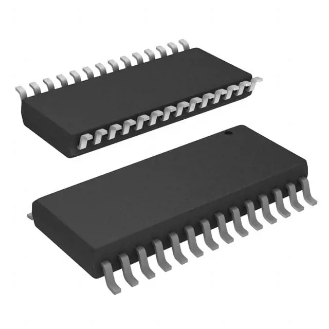
Bilder sind nur zur Referenz
CY62256NLL-70SNXC
IC SRAM 256KBIT PARALLEL 28SOIC
- Hersteller
- Fr. Teil #CY62256NLL-70SNXC
- Paket SOIC-28
- Datenblatt CY62256NLL-70SNXC DataSheet
- Auf Lager3703
100% Original und Neu
24 Stunden bereit zum Versand
365 Tage Garantie
RFQ & Erhalten Sie mehr Rabatte
Spezifikationen
| Package | Tube |
| Series | MoBL® |
| ProductStatus | Obsolete |
| MemoryType | Volatile |
| MemoryFormat | SRAM |
| Technology | SRAM - Asynchronous |
| MemorySize | 256Kb (32K x 8) |
| MemoryInterface | Parallel |
| WriteCycleTime-WordPage | 70ns |
| AccessTime | 70 ns |
| Voltage-Supply | 4.5V ~ 5.5V |
| OperatingTemperature | 0°C ~ 70°C (TA) |
| MountingType | Surface Mount |
| Package/Case | 28-SOIC (0.295, 7.50mm Width) |
Übersicht
Description
This SRAM is organized in a 32K x 8 configuration, meaning it has 32,768 addressable locations, each capable of storing 8 bits of data. It uses a CMOS technology, which contributes to its low power consumption and high reliability.
The CY62256NLL-70SNXC is commonly used in various applications, including cache memory, data buffer storage, and embedded systems where speed and power efficiency are critical. Its easy integration into existing systems makes it a popular choice among designers. The package type is typically a 28-pin SOIC, providing a compact form factor for space-constrained designs.
Features
Key features include:
- Low operating voltage: Typically 3.0V to 3.6V, supporting battery-operated devices.
- Asynchronous operation: Eliminates the need for external clock signals, simplifying system design.
- High-speed access: Provides quick data access, enhancing overall system performance.
- Data retention: Retains data without refresh cycles, making it suitable for various applications.
- Wide operating temperature range: Ensures reliability in diverse environments.
These characteristics make the CY62256NLL-70SNXC a popular choice for consumer electronics, telecommunications, and industrial applications.
Package
Pinout
Pin Functions:
1. A0-A14: Address inputs (15 bits) to access memory locations.
2. D0-D7: Data inputs/outputs (8 bits) for reading/writing data.
3. CE: Chip Enable - activates the memory chip when low.
4. OE: Output Enable - controls the output; active when low.
5. WE: Write Enable - controls write operations; active when low.
6. VCC: Power Supply - typically +3V to +5V.
7. GND: Ground.
The chip is used in applications requiring fast access times and low power consumption.
Manufacturer
Application
Equivalent
Versand
VersandmethodenWir
bieten Sie globale Versanddienstleistungen durch DHL, FedEx, TNT, UPS oder einen anderen Spediteur Ihrer Wahl.
Versandgebührenreferenz (DHL/FedEx):
DHL: Versandkosten reichen von $25-$45 (0.5kg), mit einer geschätzten Lieferzeit von 2-5 Werktagen.
von FedEx: Versandkosten reichen von $25-$40 (0.5kg), mit einer geschätzten Lieferzeit von 3-7 Werktagen.
UPS: Versandkosten reichen von $25-$45 (0.5kg), mit einer geschätzten Lieferzeit von 3-7 Werktagen.
TNT: Versandkosten reichen von $25-$65 (0.5kg), mit einer geschätzten Lieferzeit von 3-7 Werktagen.
EMS: Versandkosten reichen von $30-$50 (0.5kg), mit einer geschätzten Lieferzeit von 7-15 Werktagen.
Registrierte Luftpost: Versandkosten sind $ 2- $ 4 (0,1 kg), mit einer geschätzten Lieferzeit von 5-20 Werktagen.
Zahlungen
Payment Methods
Die Zahlungsfrist ist 100% Prepaid.
Derzeit akzeptieren wir nur die folgenden Zahlungsmethoden:
1. PayPal
2. Kredit- / Debitkarte
3. Überweisung
Ähnliche
-
![MX25R8035FM1IL0]() MX25R8035FM1IL0
Macronix
-
![MX29F400CBTI-70G]() MX29F400CBTI-70G
Macronix
-
![MX25V4035FZUI]() MX25V4035FZUI
Macronix
-
![MX30LF2G28AD-TI]() MX30LF2G28AD-TI
Macronix
-
![MX25L8035EM2I-10G]() MX25L8035EM2I-10G
Macronix
-
![MX25V1635FM2I]() MX25V1635FM2I
Macronix
-
![MX25L12833FM2I-10G]() MX25L12833FM2I-10..
Macronix
-
![MX25L12833FZ2I-10G]() MX25L12833FZ2I-10..
Macronix
-
![MX25L12833FZNI-10G]() MX25L12833FZNI-10..
Macronix
-
![MX29F040CQI-70G]() MX29F040CQI-70G
Macronix
-
![MX25L25645GXDI-08G]() MX25L25645GXDI-08..
Macronix
-
![MX30LF4G18AC-TI]() MX30LF4G18AC-TI
Macronix