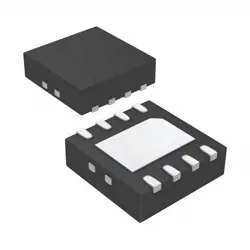
Bilder sind nur zur Referenz
CY7C1041CV33-10BAXE
IC SRAM 4MBIT PARALLEL 48FBGA
- Hersteller
- Fr. Teil #CY7C1041CV33-10BAXE
- Paket
- Datenblatt CY7C1041CV33-10BAXE DataSheet
- Auf Lager4541
100% Original und Neu
24 Stunden bereit zum Versand
365 Tage Garantie
RFQ & Erhalten Sie mehr Rabatte
Spezifikationen
| Part Status | Discontinued at Digi-Key |
| DigiKey Programmable | Not Verified |
| Memory Type | Volatile |
| Memory Format | SRAM |
| Technology | SRAM - Asynchronous |
| Memory Size | 4Mbit |
| Memory Organization | 256K x 16 |
| Memory Interface | Parallel |
| Write Cycle Time - Word, Page | 10ns |
| Voltage - Supply | 3V ~ 3.6V |
| Operating Temperature | -40°C ~ 125°C (TA) |
| Mounting Type | Surface Mount |
| Package / Case | 48-TFBGA |
| Supplier Device Package | 48-FBGA (7x8.5) |
| Base Product Number | CY7C1041 |
| Access Time | 10 ns |
Übersicht
Description
Features
Key features include:
- 4Mb density organized as 512K x 8.
- Operates at 3.3V for lower power consumption.
- Fast access time of 10ns, suitable for high-speed operations.
- CMOS technology for low power and high reliability.
- Vcc tolerance and data retention at low voltage.
- Input and output directly TTL compatible.
- Automatic power-down feature for reduced power consumption when deselected.
This SRAM is suitable for a variety of applications including industrial, automotive, and consumer electronics, where rapid data access and low power usage are critical. Its compact TSOP package design also enables efficient use of space in electronic assemblies.
Package
Pinout
In terms of pin count, the CY7C1041CV33-10BAXE comes in a 44-pin TSOP II package. Its primary function is to provide fast and reliable data storage and retrieval, typically used in applications requiring quick access to data, such as caches, buffers, and temporary data storage in various digital systems.
Key functions of the pins include:
- Address lines to select memory locations.
- Data input/output lines for reading and writing data.
- Control pins for operations such as chip enable (CE), write enable (WE), and output enable (OE).
- Power and ground pins to power the device.
This chip is particularly well-suited for use in applications requiring high-speed data access and storage efficiency.
Manufacturer
Application
Equivalent
1. ISSI IS61WV25616EDBLL
2. Alliance Memory AS7C34098A-10BIN
3. Renesas (formerly IDT) 71V416S10PHG
When seeking equivalents, ensure compatibility in terms of pin configuration, speed, power supply voltage, and operating temperature range. Always verify the datasheet details to ensure full compatibility with your application.
Versand
VersandmethodenWir
bieten Sie globale Versanddienstleistungen durch DHL, FedEx, TNT, UPS oder einen anderen Spediteur Ihrer Wahl.
Versandgebührenreferenz (DHL/FedEx):
DHL: Versandkosten reichen von $25-$45 (0.5kg), mit einer geschätzten Lieferzeit von 2-5 Werktagen.
von FedEx: Versandkosten reichen von $25-$40 (0.5kg), mit einer geschätzten Lieferzeit von 3-7 Werktagen.
UPS: Versandkosten reichen von $25-$45 (0.5kg), mit einer geschätzten Lieferzeit von 3-7 Werktagen.
TNT: Versandkosten reichen von $25-$65 (0.5kg), mit einer geschätzten Lieferzeit von 3-7 Werktagen.
EMS: Versandkosten reichen von $30-$50 (0.5kg), mit einer geschätzten Lieferzeit von 7-15 Werktagen.
Registrierte Luftpost: Versandkosten sind $ 2- $ 4 (0,1 kg), mit einer geschätzten Lieferzeit von 5-20 Werktagen.
Zahlungen
Payment Methods
Die Zahlungsfrist ist 100% Prepaid.
Derzeit akzeptieren wir nur die folgenden Zahlungsmethoden:
1. PayPal
2. Kredit- / Debitkarte
3. Überweisung
Ähnliche
-
![MX25R8035FM1IL0]() MX25R8035FM1IL0
MX25R8035FM1IL0
Macronix
-
![MX25V1635FZNQ03]() MX25V1635FZNQ03
MX25V1635FZNQ03
Macronix
-
![MX29F400CBTI-70G]() MX29F400CBTI-70G
MX29F400CBTI-70G
Macronix
-
![MX25L25673GMI-08G]() MX25L25673GMI-08G
MX25L25673GMI-08G
Macronix
-
![MX25L12833FM2I-10G]() MX25L12833FM2I-10..
MX25L12833FM2I-10..
Macronix
-
![MX25L12833FZ2I-10G]() MX25L12833FZ2I-10..
MX25L12833FZ2I-10..
Macronix
-
![MX25L12833FZNI-10G]() MX25L12833FZNI-10..
MX25L12833FZNI-10..
Macronix
-
![MX25U25645GXDI00]() MX25U25645GXDI00
MX25U25645GXDI00
Macronix
-
![MX29F800CBTI-70G]() MX29F800CBTI-70G
MX29F800CBTI-70G
Macronix
-
![MX25L1006EMI-10G]() MX25L1006EMI-10G
MX25L1006EMI-10G
Macronix
-
![MX25L4006EM2I-12G]() MX25L4006EM2I-12G
MX25L4006EM2I-12G
Macronix
-
![MX25R4035FM1IL0]() MX25R4035FM1IL0
MX25R4035FM1IL0
Macronix