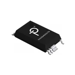
Bilder sind nur zur Referenz
EF2L45BG256B
- Hersteller
- Fr. Teil #EF2L45BG256B
- Paket
- Datenblatt
- Auf Lager20800
100% Original und Neu
24 Stunden bereit zum Versand
365 Tage Garantie
RFQ & Erhalten Sie mehr Rabatte
Spezifikationen
| Manufacturer | JLCPCB Assembly |
| Package | FBGA-256 |
Übersicht
Description
This memory chip is based on advanced 3D NAND technology, enabling higher data density, improved durability, and faster read/write speeds compared to traditional 2D NAND solutions. It supports features such as error correction, wear leveling, and power loss protection, enhancing data integrity and longevity.
The EF2L45BG256B interfaces through standard protocols like ONFI or Toggle Mode, ensuring compatibility with various controllers and systems. Its versatility makes it suitable for use in smartphones, tablets, embedded systems, and other high-demand environments where reliable and efficient data storage is essential. Overall, the EF2L45BG256B represents a modern solution for expanding memory capabilities in a wide range of electronic applications.
Features
1. Organization: It is organized as 2048 blocks of 128 pages, with each page consisting of 2048 bytes of user data plus additional spare areas for error correction.
2. Interface: The device utilizes a parallel interface, allowing for easy integration into various systems.
3. High Performance: Supports fast read and write speeds, enhancing overall data transfer efficiency.
4. Reliability: Features advanced error correction capabilities and wear leveling to extend the lifespan of the memory.
5. Low Power Consumption: Designed for energy efficiency, making it suitable for battery-operated devices.
6. Temperature Range: Operates over a wide temperature range, ensuring functionality in diverse environments.
7. Applications: Ideal for use in consumer electronics, automotive, and industrial applications requiring reliable data storage.
These features make the EF2L45BG256B a versatile choice for modern digital storage solutions.
Package
Pinout
The primary functions of the pins include:
1. Data Inputs/Outputs (DQ): 8 bits for data transfer.
2. Address Inputs (A): Used to select the memory location.
3. Control Pins (CS, RAS, CAS, WE): For controlling read and write operations.
4. Clock Input (CK): Synchronization for data transfer.
5. Power Supply (VDD, VSS): Power connections for the device.
6. Mode Register Set (MRS) and Refresh Pins: For setting operational modes and refreshing the memory.
This device supports a wide range of functionalities, including burst read/write operations, and is designed for high performance in various applications.
Manufacturer
Application
Equivalent
Versand
VersandmethodenWir
bieten Sie globale Versanddienstleistungen durch DHL, FedEx, TNT, UPS oder einen anderen Spediteur Ihrer Wahl.
Versandgebührenreferenz (DHL/FedEx):
DHL: Versandkosten reichen von $25-$45 (0.5kg), mit einer geschätzten Lieferzeit von 2-5 Werktagen.
von FedEx: Versandkosten reichen von $25-$40 (0.5kg), mit einer geschätzten Lieferzeit von 3-7 Werktagen.
UPS: Versandkosten reichen von $25-$45 (0.5kg), mit einer geschätzten Lieferzeit von 3-7 Werktagen.
TNT: Versandkosten reichen von $25-$65 (0.5kg), mit einer geschätzten Lieferzeit von 3-7 Werktagen.
EMS: Versandkosten reichen von $30-$50 (0.5kg), mit einer geschätzten Lieferzeit von 7-15 Werktagen.
Registrierte Luftpost: Versandkosten sind $ 2- $ 4 (0,1 kg), mit einer geschätzten Lieferzeit von 5-20 Werktagen.
Zahlungen
Payment Methods
Die Zahlungsfrist ist 100% Prepaid.
Derzeit akzeptieren wir nur die folgenden Zahlungsmethoden:
1. PayPal
2. Kredit- / Debitkarte
3. Überweisung
Ähnliche
-
![MX25V1635FZNQ03]() MX25V1635FZNQ03
MX25V1635FZNQ03
Macronix
-
![MX66U1G45GXDI00]() MX66U1G45GXDI00
MX66U1G45GXDI00
Macronix
-
![MX25V5126FM1I]() MX25V5126FM1I
MX25V5126FM1I
Macronix
-
![MX25V4035FZUI]() MX25V4035FZUI
MX25V4035FZUI
Macronix
-
![MX30LF2G28AD-TI]() MX30LF2G28AD-TI
MX30LF2G28AD-TI
Macronix
-
![MX25L25673GMI-08G]() MX25L25673GMI-08G
MX25L25673GMI-08G
Macronix
-
![MX25L2006EM1I-12G]() MX25L2006EM1I-12G
MX25L2006EM1I-12G
Macronix
-
![MX25U25645GXDI00]() MX25U25645GXDI00
MX25U25645GXDI00
Macronix
-
![MX29LV160DTTI-70G]() MX29LV160DTTI-70G
MX29LV160DTTI-70G
Macronix
-
![MX29F800CBTI-70G]() MX29F800CBTI-70G
MX29F800CBTI-70G
Macronix
-
![MX25L1006EMI-10G]() MX25L1006EMI-10G
MX25L1006EMI-10G
Macronix
-
![MX66U1G45GMI00]() MX66U1G45GMI00
MX66U1G45GMI00
Macronix