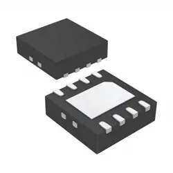
Bilder sind nur zur Referenz
EPCQL512F24IN
IC QUAD-SERIAL LOW VOLTAGE CONFI
- Hersteller
- Fr. Teil #EPCQL512F24IN
- Paket 24-TBGA
- Datenblatt
- Auf Lager2397
100% Original und Neu
24 Stunden bereit zum Versand
365 Tage Garantie
RFQ & Erhalten Sie mehr Rabatte
Spezifikationen
| Package | Tray |
| Series | EPCQ-L |
| ProductStatus | Obsolete |
| ProgrammableType | In System Programmable |
| MemorySize | 512Mb |
| Voltage-Supply | 1.7V ~ 2V |
| OperatingTemperature | -40°C ~ 85°C |
| MountingType | Surface Mount |
| Package/Case | 24-TBGA |
Übersicht
Description
Key characteristics of the EPCQL512F24IN include its high-speed read and write capabilities, low power consumption, and durability, making it suitable for a variety of applications, including mobile devices and automotive systems. The chip typically supports various data transfer modes and is compatible with established NAND protocols, ensuring ease of integration into existing electronic designs.
In summary, the EPCQL512F24IN is a versatile and efficient memory solution tailored for modern electronic devices, offering both performance and reliability.
Features
1. Storage Capacity: 512 Kbits organized in 64K x 8 bits.
2. Interface: Serial interface for easy integration.
3. Operating Voltage: Typically operates within a voltage range of 2.7V to 5.5V.
4. Data Retention: Offers long data retention, typically up to 100 years.
5. Write Endurance: Supports a minimum of 100,000 write/erase cycles per cell.
6. Fast Programming: Quick write times enhance overall performance.
7. Low Power Consumption: Ideal for battery-operated devices.
8. Temperature Range: Operates effectively in a wide temperature range, accommodating various applications.
These features make the EPCQL512F24IN suitable for applications in consumer electronics, automotive, and industrial sectors where reliable data storage is critical.
Package
Pinout
### Pin Count:
- Total Pins: 24
### Functions of Pins:
1. Power Supply Pins:
- VCC: Power supply for the device.
- GND: Ground reference.
2. Data Interface Pins:
- DQ0 to DQ7: Data input/output pins for serial communication.
3. Control Pins:
- CS (Chip Select): Activates the device for communication.
- SCK (Serial Clock): Clock signal for synchronous data transmission.
- MOSI (Master Out Slave In): Data input pin.
- MISO (Master In Slave Out): Data output pin.
4. Additional Functions:
- WP (Write Protect): Protects the memory from accidental writes.
- RESET: Resets the device.
This device typically supports commands for reading, writing, and erasing data, making it suitable for various applications requiring non-volatile storage.
Manufacturer
Application
Equivalent
Versand
VersandmethodenWir
bieten Sie globale Versanddienstleistungen durch DHL, FedEx, TNT, UPS oder einen anderen Spediteur Ihrer Wahl.
Versandgebührenreferenz (DHL/FedEx):
DHL: Versandkosten reichen von $25-$45 (0.5kg), mit einer geschätzten Lieferzeit von 2-5 Werktagen.
von FedEx: Versandkosten reichen von $25-$40 (0.5kg), mit einer geschätzten Lieferzeit von 3-7 Werktagen.
UPS: Versandkosten reichen von $25-$45 (0.5kg), mit einer geschätzten Lieferzeit von 3-7 Werktagen.
TNT: Versandkosten reichen von $25-$65 (0.5kg), mit einer geschätzten Lieferzeit von 3-7 Werktagen.
EMS: Versandkosten reichen von $30-$50 (0.5kg), mit einer geschätzten Lieferzeit von 7-15 Werktagen.
Registrierte Luftpost: Versandkosten sind $ 2- $ 4 (0,1 kg), mit einer geschätzten Lieferzeit von 5-20 Werktagen.
Zahlungen
Payment Methods
Die Zahlungsfrist ist 100% Prepaid.
Derzeit akzeptieren wir nur die folgenden Zahlungsmethoden:
1. PayPal
2. Kredit- / Debitkarte
3. Überweisung
Ähnliche
-
![MX25V4035FZUI]() MX25V4035FZUI
MX25V4035FZUI
Macronix
-
![MX25V2033FM1I]() MX25V2033FM1I
MX25V2033FM1I
Macronix
-
![MX25R3235FZNIL0]() MX25R3235FZNIL0
MX25R3235FZNIL0
Macronix
-
![MX25V16066M2I02]() MX25V16066M2I02
MX25V16066M2I02
Macronix
-
![MX25R6435FBDIL0]() MX25R6435FBDIL0
MX25R6435FBDIL0
Macronix
-
![MX25L12833FM2I-10G]() MX25L12833FM2I-10..
MX25L12833FM2I-10..
Macronix
-
![MX25L12833FZNI-10G]() MX25L12833FZNI-10..
MX25L12833FZNI-10..
Macronix
-
![MX25L12835FZ2I-10G]() MX25L12835FZ2I-10..
MX25L12835FZ2I-10..
Macronix
-
![MX29LV160DTTI-70G]() MX29LV160DTTI-70G
MX29LV160DTTI-70G
Macronix
-
![MX30LF4G18AC-TI]() MX30LF4G18AC-TI
MX30LF4G18AC-TI
Macronix
-
![MX25U51245GZ4I00]() MX25U51245GZ4I00
MX25U51245GZ4I00
Macronix
-
![MX25L1006EMI-10G]() MX25L1006EMI-10G
MX25L1006EMI-10G
Macronix