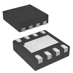
Bilder sind nur zur Referenz
FDC6321C
DUAL N & P CHANNEL DIGITAL FET 2
- Hersteller
- Fr. Teil #FDC6321C
- Paket
- Datenblatt FDC6321C DataSheet
- Auf Lager3361
100% Original und Neu
24 Stunden bereit zum Versand
365 Tage Garantie
RFQ & Erhalten Sie mehr Rabatte
Spezifikationen
| Supplier | Rochester Electronics, LLC |
| Package | Bulk |
| ProductStatus | Active |
Übersicht
Description
Key features of the FDC6321C include low power consumption, fast response times, and robust temperature performance, making it suitable for applications in motor control, sensor signal conditioning, and audio systems. Its dual-channel architecture allows for simultaneous output generation, enhancing its versatility in complex applications. Overall, the FDC6321C is ideal for engineers seeking a reliable and efficient DAC solution for various electronic designs.
Features
- Dual-Channel Input: Supports simultaneous sampling of two channels.
- 12-bit Resolution: Provides accurate digital representation of analog signals.
- Sampling Rate: Capable of sampling rates up to 1 MSPS (megasample per second).
- Low Power Consumption: Optimized for battery-operated devices with low quiescent current.
- Integrated Voltage Reference: Reduces external component count and simplifies design.
- SPI Interface: Facilitates easy communication with microcontrollers and digital signal processors.
- Programmable Gain Amplifier (PGA): Allows for signal conditioning and dynamic range optimization.
- Temperature Range: Suitable for industrial applications with a wide operating temperature range.
These features make the FDC6321C ideal for applications such as industrial automation, medical instrumentation, and portable measurement devices.
Package
Pinout
The pin functions are as follows:
1. VDD: Power supply input.
2. GND: Ground connection.
3. PHASE: Connection to the switch node.
4. BOOT: Bootstrap capacitor connection for high-side gate drive.
5. HS: High-side gate drive output.
6. LS: Low-side gate drive output.
7. EN: Enable pin to turn on the driver.
8. COMP: Compensation pin for stability in feedback control.
9. CSN: Current sense negative terminal.
10. CSP: Current sense positive terminal.
The device is used in power management applications, providing efficient control of MOSFETs in DC-DC converters.
Manufacturer
Application
Equivalent
Versand
VersandmethodenWir
bieten Sie globale Versanddienstleistungen durch DHL, FedEx, TNT, UPS oder einen anderen Spediteur Ihrer Wahl.
Versandgebührenreferenz (DHL/FedEx):
DHL: Versandkosten reichen von $25-$45 (0.5kg), mit einer geschätzten Lieferzeit von 2-5 Werktagen.
von FedEx: Versandkosten reichen von $25-$40 (0.5kg), mit einer geschätzten Lieferzeit von 3-7 Werktagen.
UPS: Versandkosten reichen von $25-$45 (0.5kg), mit einer geschätzten Lieferzeit von 3-7 Werktagen.
TNT: Versandkosten reichen von $25-$65 (0.5kg), mit einer geschätzten Lieferzeit von 3-7 Werktagen.
EMS: Versandkosten reichen von $30-$50 (0.5kg), mit einer geschätzten Lieferzeit von 7-15 Werktagen.
Registrierte Luftpost: Versandkosten sind $ 2- $ 4 (0,1 kg), mit einer geschätzten Lieferzeit von 5-20 Werktagen.
Zahlungen
Payment Methods
Die Zahlungsfrist ist 100% Prepaid.
Derzeit akzeptieren wir nur die folgenden Zahlungsmethoden:
1. PayPal
2. Kredit- / Debitkarte
3. Überweisung
Ähnliche
-
![MX25R8035FM1IL0]() MX25R8035FM1IL0
MX25R8035FM1IL0
Macronix
-
![MX29F400CBTI-70G]() MX29F400CBTI-70G
MX29F400CBTI-70G
Macronix
-
![MX66U1G45GXDI00]() MX66U1G45GXDI00
MX66U1G45GXDI00
Macronix
-
![MX25V4035FZUI]() MX25V4035FZUI
MX25V4035FZUI
Macronix
-
![MX25V16066M1I02]() MX25V16066M1I02
MX25V16066M1I02
Macronix
-
![MX30LF2G28AD-TI]() MX30LF2G28AD-TI
MX30LF2G28AD-TI
Macronix
-
![MX25L8035EM2I-10G]() MX25L8035EM2I-10G
MX25L8035EM2I-10G
Macronix
-
![MX25R6435FBDIL0]() MX25R6435FBDIL0
MX25R6435FBDIL0
Macronix
-
![MX25L25673GMI-08G]() MX25L25673GMI-08G
MX25L25673GMI-08G
Macronix
-
![MX25L25673GMI-10G]() MX25L25673GMI-10G
MX25L25673GMI-10G
Macronix
-
![MX25U3232FZBI02]() MX25U3232FZBI02
MX25U3232FZBI02
Macronix
-
![MX25L6433FM2I-08G]() MX25L6433FM2I-08G
MX25L6433FM2I-08G
Macronix