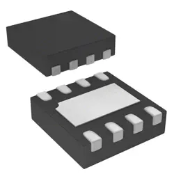
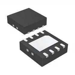
Bilder sind nur zur Referenz
FDC653N
MOSFET N-CH 30V 5A SUPERSOT6
- Hersteller
- Fr. Teil #FDC653N
- Paket SSOT-6
- Datenblatt FDC653N DataSheet
- Auf Lager3192
100% Original und Neu
24 Stunden bereit zum Versand
365 Tage Garantie
RFQ & Erhalten Sie mehr Rabatte
Spezifikationen
| Package | Tape & Reel (TR),Cut Tape (CT) |
| ProductStatus | Active |
| FETType | N-Channel |
| Technology | MOSFET (Metal Oxide) |
| DraintoSourceVoltage(Vdss) | 30 V |
| Current-ContinuousDrain(Id)@25°C | 5A (Ta) |
| DriveVoltage(MaxRdsOnMinRdsOn) | 4.5V, 10V |
| RdsOn(Max)@IdVgs | 35mOhm @ 5A, 10V |
| Vgs(th)(Max)@Id | 2V @ 250µA |
| GateCharge(Qg)(Max)@Vgs | 17 nC @ 10 V |
| Vgs(Max) | ±20V |
| InputCapacitance(Ciss)(Max)@Vds | 350 pF @ 15 V |
| PowerDissipation(Max) | 1.6W (Ta) |
| OperatingTemperature | -55°C ~ 150°C (TJ) |
| MountingType | Surface Mount |
| SupplierDevicePackage | SuperSOT™-6 |
Übersicht
Description
The FDC653N also integrates several protection features, including overcurrent protection, thermal shutdown, and short-circuit protection, enhancing its reliability in demanding environments. Its compact package options facilitate easy integration into space-constrained designs. Overall, the FDC653N is suitable for applications in consumer electronics, automotive, and industrial systems, where stable and efficient voltage regulation is crucial.
Features
1. Voltage Rating: It typically has a maximum drain-source voltage (Vds) of around 30V, making it suitable for low-voltage applications.
2. Current Rating: The device can handle drain current (Id) up to 24A, allowing it to manage significant load demands.
3. Rds(on): It boasts a low on-resistance (Rds(on)), often around 10.5 mΩ, which reduces power losses and enhances efficiency.
4. Gate Threshold Voltage: The gate threshold voltage (Vgs(th)) typically ranges from 1V to 3V, facilitating easier driving with logic-level signals.
5. Package: Available in a DPAK or similar package, offering good thermal performance and ease of mounting.
6. Fast Switching Speed: Suitable for high-frequency applications due to its fast switching capabilities.
7. Applications: Commonly used in power management, DC-DC converters, and motor control circuits.
Overall, the FDC653N is a versatile MOSFET ideal for a variety of electronic applications needing efficient power management.
Package
Pinout
1. Gate 1 (G1) - Controls the switching of the first N-channel MOSFET.
2. Drain 1 (D1) - The output connected to the load for the first MOSFET.
3. Source 1 (S1) - Source terminal for the first MOSFET, typically connected to ground in low-side switching applications.
4. Gate 2 (G2) - Controls the switching of the second N-channel MOSFET.
5. Drain 2 (D2) - The output connected to the load for the second MOSFET.
The FDC653N is used in various applications, including power management, motor control, and switching circuits, due to its low on-resistance and high-speed switching capabilities.
Manufacturer
Application
Equivalent
Versand
VersandmethodenWir
bieten Sie globale Versanddienstleistungen durch DHL, FedEx, TNT, UPS oder einen anderen Spediteur Ihrer Wahl.
Versandgebührenreferenz (DHL/FedEx):
DHL: Versandkosten reichen von $25-$45 (0.5kg), mit einer geschätzten Lieferzeit von 2-5 Werktagen.
von FedEx: Versandkosten reichen von $25-$40 (0.5kg), mit einer geschätzten Lieferzeit von 3-7 Werktagen.
UPS: Versandkosten reichen von $25-$45 (0.5kg), mit einer geschätzten Lieferzeit von 3-7 Werktagen.
TNT: Versandkosten reichen von $25-$65 (0.5kg), mit einer geschätzten Lieferzeit von 3-7 Werktagen.
EMS: Versandkosten reichen von $30-$50 (0.5kg), mit einer geschätzten Lieferzeit von 7-15 Werktagen.
Registrierte Luftpost: Versandkosten sind $ 2- $ 4 (0,1 kg), mit einer geschätzten Lieferzeit von 5-20 Werktagen.
Zahlungen
Payment Methods
Die Zahlungsfrist ist 100% Prepaid.
Derzeit akzeptieren wir nur die folgenden Zahlungsmethoden:
1. PayPal
2. Kredit- / Debitkarte
3. Überweisung
Ähnliche
-
![MX25R8035FM1IL0]() MX25R8035FM1IL0
MX25R8035FM1IL0
Macronix
-
![MX29F400CBTI-70G]() MX29F400CBTI-70G
MX29F400CBTI-70G
Macronix
-
![MX25V5126FM1I]() MX25V5126FM1I
MX25V5126FM1I
Macronix
-
![MX25V4035FZUI]() MX25V4035FZUI
MX25V4035FZUI
Macronix
-
![MX25V2033FM1I]() MX25V2033FM1I
MX25V2033FM1I
Macronix
-
![MX25V16066M1I02]() MX25V16066M1I02
MX25V16066M1I02
Macronix
-
![MX25V16066M2I02]() MX25V16066M2I02
MX25V16066M2I02
Macronix
-
![MX30LF2G28AD-TI]() MX30LF2G28AD-TI
MX30LF2G28AD-TI
Macronix
-
![MX29GL512FHXFI-11G]() MX29GL512FHXFI-11..
MX29GL512FHXFI-11..
Macronix
-
![MX25R1635FZUIH0]() MX25R1635FZUIH0
MX25R1635FZUIH0
Macronix
-
![MX25L12833FM2I-10G]() MX25L12833FM2I-10..
MX25L12833FM2I-10..
Macronix
-
![MX25L12833FZNI-10G]() MX25L12833FZNI-10..
MX25L12833FZNI-10..
Macronix