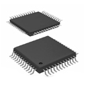

Bilder sind nur zur Referenz
GD25S512MD
NOR Flash 3.3V Uniform Sector Dual and Q
- Hersteller
- Fr. Teil #GD25S512MD
- Paket
- Datenblatt GD25S512MD DataSheet
- Auf Lager10792
100% Original und Neu
24 Stunden bereit zum Versand
365 Tage Garantie
RFQ & Erhalten Sie mehr Rabatte
Spezifikationen
Übersicht
Description
This memory device is ideal for embedded systems, IoT applications, and consumer electronics, providing features such as low power consumption, uniform memory block architecture, and multiple read modes. It supports various programming and erasing methods, including sector and chip erase, enhancing flexibility for developers.
The GD25S512MD is built to operate within a temperature range of -40°C to +85°C, making it suitable for industrial applications. Its compact package options allow for efficient space utilization on PCBs. Overall, the GD25S512MD is a reliable choice for applications needing durable, high-capacity non-volatile storage.
Features
1. Interface: Supports SPI protocol, compatible with standard, dual, and quad modes for high-speed data transfer.
2. Memory Density: 512 Mbit capacity, organized as 64M x 8 bits.
3. Speed: Operates at a clock frequency of up to 104 MHz in quad SPI mode.
4. Data Retention: Offers a minimum data retention of 20 years.
5. Endurance: Supports up to 100,000 program/erase cycles per sector.
6. Block Architecture: Contains multiple sectors (typically 4 KB, 32 KB, or 64 KB) for flexible memory management and efficient data storage.
7. Power Supply: Operates on a voltage range of 2.7V to 3.6V.
8. Package Options: Available in various packages, including WSON, SOIC, and DFN for compact designs.
This chip is ideal for applications in consumer electronics, automotive, and industrial systems where non-volatile storage is required.
Package
Pinout
1. CS (Chip Select) – Active low input to select the device.
2. SO (Serial Output) – Data output for read operations.
3. WP (Write Protect) – Input to protect the memory from accidental writes.
4. VSS (Ground) – Ground connection.
5. SCK (Serial Clock) – Clock input for synchronous communication.
6. SI (Serial Input) – Data input for write operations.
7. HOLD – Input to pause operations without resetting the device.
8. VCC – Power supply connection.
Additional pins may be present for specific functionality, such as additional ground or power connections. The device supports various modes of operation, including Quad SPI, allowing for high-speed data transfer.
Manufacturer
Application
Equivalent
1. Winbond W25Q512JV
2. Microchip SST26VF512
3. Spansion S25FL512S
4. Macronix MX25L51245G
These alternatives offer similar specifications and interfaces, but it's important to verify specific features and compatibility for your application.
Versand
VersandmethodenWir
bieten Sie globale Versanddienstleistungen durch DHL, FedEx, TNT, UPS oder einen anderen Spediteur Ihrer Wahl.
Versandgebührenreferenz (DHL/FedEx):
DHL: Versandkosten reichen von $25-$45 (0.5kg), mit einer geschätzten Lieferzeit von 2-5 Werktagen.
von FedEx: Versandkosten reichen von $25-$40 (0.5kg), mit einer geschätzten Lieferzeit von 3-7 Werktagen.
UPS: Versandkosten reichen von $25-$45 (0.5kg), mit einer geschätzten Lieferzeit von 3-7 Werktagen.
TNT: Versandkosten reichen von $25-$65 (0.5kg), mit einer geschätzten Lieferzeit von 3-7 Werktagen.
EMS: Versandkosten reichen von $30-$50 (0.5kg), mit einer geschätzten Lieferzeit von 7-15 Werktagen.
Registrierte Luftpost: Versandkosten sind $ 2- $ 4 (0,1 kg), mit einer geschätzten Lieferzeit von 5-20 Werktagen.
Zahlungen
Payment Methods
Die Zahlungsfrist ist 100% Prepaid.
Derzeit akzeptieren wir nur die folgenden Zahlungsmethoden:
1. PayPal
2. Kredit- / Debitkarte
3. Überweisung
Ähnliche
-
![MX25L3233FM1I-08Q]() MX25L3233FM1I-08Q
Macronix
-
![MX29F400CBTI-70G]() MX29F400CBTI-70G
Macronix
-
![MX25V4035FZUI]() MX25V4035FZUI
Macronix
-
![MX25V2033FM1I]() MX25V2033FM1I
Macronix
-
![MX25R3235FZNIL0]() MX25R3235FZNIL0
Macronix
-
![MX30LF2G28AD-TI]() MX30LF2G28AD-TI
Macronix
-
![MX25R6435FBDIL0]() MX25R6435FBDIL0
Macronix
-
![MX25L25673GMI-08G]() MX25L25673GMI-08G
Macronix
-
![MX25L25673GMI-10G]() MX25L25673GMI-10G
Macronix
-
![MX25U51279GXDR00]() MX25U51279GXDR00
Macronix
-
![MX25U25643GZNI00]() MX25U25643GZNI00
Macronix
-
![MX25U6435FM2I-10G]() MX25U6435FM2I-10G
Macronix