Bilder sind nur zur Referenz
HEF4011BT
Logic Gates
- Hersteller
- Fr. Teil #HEF4011BT
- Paket
- Datenblatt
- Auf Lager5679
100% Original und Neu
24 Stunden bereit zum Versand
365 Tage Garantie
RFQ & Erhalten Sie mehr Rabatte
Spezifikationen
Übersicht
Description
This IC is known for its low power consumption, high noise immunity, and compatibility with other CMOS devices. It is commonly used in digital logic circuits, signal processing, and switching applications. The package typically features a DIP (Dual In-line Package) or surface mount options, making it suitable for prototyping and production.
In summary, the HEF4011BT is essential for implementing NAND logic functions in electronic designs, providing flexibility and efficiency in various applications.
Features
1. Quad NAND Gates: Contains four independent two-input NAND gates.
2. Wide Supply Voltage Range: Operates from 3V to 15V, making it versatile for various applications.
3. Low Power Consumption: Consumes less power compared to other logic families, enhancing energy efficiency.
4. High Noise Immunity: Offers good noise margins, ensuring reliable operation in noisy environments.
5. Complementary Output: Provides both high and low output signals, suitable for driving subsequent stages.
6. Standard Logic Levels: Compatible with standard TTL logic levels.
7. Temperature Range: Operates effectively over a wide temperature range (-40°C to +125°C).
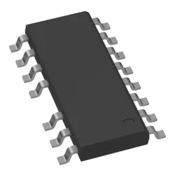
8. Package Options: Available in various package types, including DIP, SOIC, and TSSOP.
This makes the HEF4011BT suitable for digital circuits in computing, automotive, and consumer electronics applications.
Package
Pinout
1. 1A1 - Input for the first NAND gate (Input A).
2. 1B1 - Input for the first NAND gate (Input B).
3. 1Y1 - Output for the first NAND gate.
4. 2A1 - Input for the second NAND gate (Input A).
5. 2B1 - Input for the second NAND gate (Input B).
6. 2Y1 - Output for the second NAND gate.
7. GND - Ground reference.
8. 3A1 - Input for the third NAND gate (Input A).
9. 3B1 - Input for the third NAND gate (Input B).
10. 3Y1 - Output for the third NAND gate.
11. 4A1 - Input for the fourth NAND gate (Input A).
12. 4B1 - Input for the fourth NAND gate (Input B).
13. 4Y1 - Output for the fourth NAND gate.
14. VDD - Supply voltage.
This IC is commonly used in digital circuits for logic operations.
Manufacturer
Application
Equivalent
1. 74HC00
2. 74HCT00
3. CD4011
4. MC14011
These chips offer similar functionality but may have different voltage levels and specifications. Always check the datasheets for specific requirements.
Versand
VersandmethodenWir
bieten Sie globale Versanddienstleistungen durch DHL, FedEx, TNT, UPS oder einen anderen Spediteur Ihrer Wahl.
Versandgebührenreferenz (DHL/FedEx):
DHL: Versandkosten reichen von $25-$45 (0.5kg), mit einer geschätzten Lieferzeit von 2-5 Werktagen.
von FedEx: Versandkosten reichen von $25-$40 (0.5kg), mit einer geschätzten Lieferzeit von 3-7 Werktagen.
UPS: Versandkosten reichen von $25-$45 (0.5kg), mit einer geschätzten Lieferzeit von 3-7 Werktagen.
TNT: Versandkosten reichen von $25-$65 (0.5kg), mit einer geschätzten Lieferzeit von 3-7 Werktagen.
EMS: Versandkosten reichen von $30-$50 (0.5kg), mit einer geschätzten Lieferzeit von 7-15 Werktagen.
Registrierte Luftpost: Versandkosten sind $ 2- $ 4 (0,1 kg), mit einer geschätzten Lieferzeit von 5-20 Werktagen.
Zahlungen
Payment Methods
Die Zahlungsfrist ist 100% Prepaid.
Derzeit akzeptieren wir nur die folgenden Zahlungsmethoden:
1. PayPal
2. Kredit- / Debitkarte
3. Überweisung
Ähnliche
-
![MX25V16066M1I02]() MX25V16066M1I02
Macronix
-
![MX25L8035EM2I-10G]() MX25L8035EM2I-10G
Macronix
-
![MX25U51279GXDR00]() MX25U51279GXDR00
Macronix
-
![MX25L6433FM2I-08G]() MX25L6433FM2I-08G
Macronix
-
![MX25L12833FZNI-10G]() MX25L12833FZNI-10..
Macronix
-
![MX25U25645GXDI00]() MX25U25645GXDI00
Macronix
-
![MX29F800CBTI-70G]() MX29F800CBTI-70G
Macronix
-
![MX29LV640ETTI-70G]() MX29LV640ETTI-70G
Macronix
-
![MX25L25735FMI-10G]() MX25L25735FMI-10G
Macronix
-
![MX25U51245GZ4I00]() MX25U51245GZ4I00
Macronix
-
![MX25L1006EMI-10G]() MX25L1006EMI-10G
Macronix
-
![MX66U1G45GMI00]() MX66U1G45GMI00
Macronix