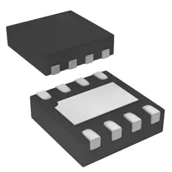
Bilder sind nur zur Referenz
IS25LQ040B-JNLE
IC FLASH 4MBIT SPI/QUAD 8SOIC
- Hersteller
- Fr. Teil #IS25LQ040B-JNLE
- Paket 8-SOIC
- Datenblatt IS25LQ040B-JNLE DataSheet
- Auf Lager3709
100% Original und Neu
24 Stunden bereit zum Versand
365 Tage Garantie
RFQ & Erhalten Sie mehr Rabatte
Spezifikationen
| Package | Bulk |
| ProductStatus | Obsolete |
| MemoryType | Non-Volatile |
| MemoryFormat | FLASH |
| Technology | FLASH - NOR |
| MemorySize | 4Mb (512K x 8) |
| MemoryInterface | SPI - Quad I/O |
| ClockFrequency | 104 MHz |
| WriteCycleTime-WordPage | 800µs |
| Voltage-Supply | 2.3V ~ 3.6V |
| OperatingTemperature | -40°C ~ 105°C (TA) |
| MountingType | Surface Mount |
| Package/Case | 8-SOIC (0.154, 3.90mm Width) |
Übersicht
Description
The IS25LQ040B supports multiple commands, including Read, Program, and Erase, along with features like dual and quad SPI modes for higher throughput. It is ideal for use in embedded systems, consumer electronics, automotive applications, and other areas where non-volatile memory is critical. Its compact package and low power consumption contribute to its popularity in various designs, particularly where space and efficiency are paramount. Overall, the IS25LQ040B-JNLE is a reliable choice for developers needing high-performance memory solutions.
Features
1. Memory Type: NOR Flash
2. Interface: SPI (Serial Peripheral Interface) with support for dual and quad I/O modes to enhance data transfer rates.
3. Density: 4 Megabits (512 Kbytes).
4. Voltage Range: Operates typically at 2.7V to 3.6V, ensuring compatibility with various low-power applications.
5. Speed: Offers fast read speeds up to 104 MHz in quad mode.
6. Endurance: Supports up to 100,000 program/erase cycles.
7. Data Retention: Provides a data retention period of up to 20 years at 25°C.
8. Package Options: Available in various packages like SOIC, WSON, and DFN.
9. Applications: Suitable for automotive, industrial, and consumer electronics, including firmware storage and code execution.
This device is ideal for applications requiring reliable, high-speed memory solutions.
Package
Pinout
1. CS# (Chip Select): Activates the device.
2. SO (Serial Output): Data output pin for read operations.
3. SIO1 (Serial Input/Output): Data input/output for dual and quad modes.
4. SI (Serial Input): Data input pin for write operations.
5. SCK (Serial Clock): Clock input for synchronizing data transfers.
6. WP# (Write Protect): Pin to protect against accidental writes.
7. HOLD#: Pauses the serial communication without resetting the device.
8. VSS: Ground reference.
This device supports standard SPI, dual, and quad modes, offering flexibility in data transfer rates and functionality for various applications.
Manufacturer
Application
Equivalent
Versand
VersandmethodenWir
bieten Sie globale Versanddienstleistungen durch DHL, FedEx, TNT, UPS oder einen anderen Spediteur Ihrer Wahl.
Versandgebührenreferenz (DHL/FedEx):
DHL: Versandkosten reichen von $25-$45 (0.5kg), mit einer geschätzten Lieferzeit von 2-5 Werktagen.
von FedEx: Versandkosten reichen von $25-$40 (0.5kg), mit einer geschätzten Lieferzeit von 3-7 Werktagen.
UPS: Versandkosten reichen von $25-$45 (0.5kg), mit einer geschätzten Lieferzeit von 3-7 Werktagen.
TNT: Versandkosten reichen von $25-$65 (0.5kg), mit einer geschätzten Lieferzeit von 3-7 Werktagen.
EMS: Versandkosten reichen von $30-$50 (0.5kg), mit einer geschätzten Lieferzeit von 7-15 Werktagen.
Registrierte Luftpost: Versandkosten sind $ 2- $ 4 (0,1 kg), mit einer geschätzten Lieferzeit von 5-20 Werktagen.
Zahlungen
Payment Methods
Die Zahlungsfrist ist 100% Prepaid.
Derzeit akzeptieren wir nur die folgenden Zahlungsmethoden:
1. PayPal
2. Kredit- / Debitkarte
3. Überweisung
Ähnliche
-
![MX25R8035FM1IL0]() MX25R8035FM1IL0
MX25R8035FM1IL0
Macronix
-
![MX66U1G45GXDI00]() MX66U1G45GXDI00
MX66U1G45GXDI00
Macronix
-
![MX25R3235FZNIL0]() MX25R3235FZNIL0
MX25R3235FZNIL0
Macronix
-
![MX30LF2G28AD-TI]() MX30LF2G28AD-TI
MX30LF2G28AD-TI
Macronix
-
![MX29GL512FHXFI-11G]() MX29GL512FHXFI-11..
MX29GL512FHXFI-11..
Macronix
-
![MX25U3232FZBI02]() MX25U3232FZBI02
MX25U3232FZBI02
Macronix
-
![MX25L12833FM2I-10G]() MX25L12833FM2I-10..
MX25L12833FM2I-10..
Macronix
-
![MX25L12835FZ2I-10G]() MX25L12835FZ2I-10..
MX25L12835FZ2I-10..
Macronix
-
![MX29F040CTI-70G]() MX29F040CTI-70G
MX29F040CTI-70G
Macronix
-
![MX29F800CBTI-70G]() MX29F800CBTI-70G
MX29F800CBTI-70G
Macronix
-
![MX25L1006EMI-10G]() MX25L1006EMI-10G
MX25L1006EMI-10G
Macronix
-
![MX30LF4G28AD-TI]() MX30LF4G28AD-TI
MX30LF4G28AD-TI
Macronix