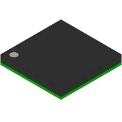
Bilder sind nur zur Referenz
IS61WV51232BLL-10BLI
IC SRAM 16MBIT PARALLEL 90TFBGA
- Hersteller
- Fr. Teil #IS61WV51232BLL-10BLI
- Paket 90-TFBGA
- Datenblatt IS61WV51232BLL-10BLI DataSheet
- Auf Lager3305
100% Original und Neu
24 Stunden bereit zum Versand
365 Tage Garantie
RFQ & Erhalten Sie mehr Rabatte
Spezifikationen
| Package | Tray |
| ProductStatus | Active |
| MemoryType | Volatile |
| MemoryFormat | SRAM |
| Technology | SRAM - Asynchronous |
| MemorySize | 16Mb (512K x 32) |
| MemoryInterface | Parallel |
| WriteCycleTime-WordPage | 10ns |
| AccessTime | 10 ns |
| Voltage-Supply | 1.65V ~ 3.6V |
| OperatingTemperature | -40°C ~ 85°C (TA) |
| MountingType | Surface Mount |
| Package/Case | 90-TFBGA |
Übersicht
Description
Key characteristics include a low voltage operation of 3.0V to 3.6V, which enhances power efficiency, along with a simple interface that supports asynchronous read and write operations. The device is packaged in a 48-pin TSOP (Thin Small Outline Package), facilitating easy integration into circuit boards.
Overall, the IS61WV51232BLL-10BLI is ideal for applications requiring fast and reliable memory solutions.
Features
1. Memory Size: 512 Kbit (64 K x 8 bits).
2. Access Time: 10 ns, allowing for fast read and write operations.
3. Operating Voltage: Typically operates at 3.0V to 3.6V, optimizing for low power consumption.
4. Asynchronous Operation: No clock required, allowing for simple control and integration into various applications.
5. Data Retention: Offers reliable data storage with low standby current.
6. Package Options: Available in various packages, including 44-pin TSOP and other surface mount configurations.
7. Temperature Range: Typically supports commercial temperature ranges, ensuring reliable performance in various environments.
This SRAM is suitable for applications in networking, telecommunications, and consumer electronics where speed and efficiency are crucial.
Package
Pinout
Key pin functions include:
- Data Pins (DQ0-DQ31): 32 data input/output pins.
- Address Pins (A0-A18): 19 address pins to select memory locations.
- Control Pins:
- CLK: Clock input for synchronous operations.
- CE: Chip Enable; activates the memory.
- WE: Write Enable; controls write operations.
- OE: Output Enable; controls data output.
- Byte Enable Pins (BE0-BE3): Control data access for each byte lane.
- Vcc: Power supply.
- GND: Ground.
This configuration allows for efficient data storage and retrieval in high-speed applications.
Manufacturer
Application
Equivalent
Versand
VersandmethodenWir
bieten Sie globale Versanddienstleistungen durch DHL, FedEx, TNT, UPS oder einen anderen Spediteur Ihrer Wahl.
Versandgebührenreferenz (DHL/FedEx):
DHL: Versandkosten reichen von $25-$45 (0.5kg), mit einer geschätzten Lieferzeit von 2-5 Werktagen.
von FedEx: Versandkosten reichen von $25-$40 (0.5kg), mit einer geschätzten Lieferzeit von 3-7 Werktagen.
UPS: Versandkosten reichen von $25-$45 (0.5kg), mit einer geschätzten Lieferzeit von 3-7 Werktagen.
TNT: Versandkosten reichen von $25-$65 (0.5kg), mit einer geschätzten Lieferzeit von 3-7 Werktagen.
EMS: Versandkosten reichen von $30-$50 (0.5kg), mit einer geschätzten Lieferzeit von 7-15 Werktagen.
Registrierte Luftpost: Versandkosten sind $ 2- $ 4 (0,1 kg), mit einer geschätzten Lieferzeit von 5-20 Werktagen.
Zahlungen
Payment Methods
Die Zahlungsfrist ist 100% Prepaid.
Derzeit akzeptieren wir nur die folgenden Zahlungsmethoden:
1. PayPal
2. Kredit- / Debitkarte
3. Überweisung
Ähnliche
-
![MX25L3233FM1I-08Q]() MX25L3233FM1I-08Q
Macronix
-
![MX25V16066M1I02]() MX25V16066M1I02
Macronix
-
![MX25R3235FZNIL0]() MX25R3235FZNIL0
Macronix
-
![MX30LF2G28AD-TI]() MX30LF2G28AD-TI
Macronix
-
![MX25L8035EM2I-10G]() MX25L8035EM2I-10G
Macronix
-
![MX25L25673GMI-10G]() MX25L25673GMI-10G
Macronix
-
![MX29GL512FHXFI-11G]() MX29GL512FHXFI-11..
Macronix
-
![MX25U51279GXDR00]() MX25U51279GXDR00
Macronix
-
![MX25R1635FZUIH0]() MX25R1635FZUIH0
Macronix
-
![MX25U25645GXDI00]() MX25U25645GXDI00
Macronix
-
![MX25L12835FZ2I-10G]() MX25L12835FZ2I-10..
Macronix
-
![MX29F040CQI-70G]() MX29F040CQI-70G
Macronix