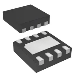
Bilder sind nur zur Referenz
KLMBG2JETD-B041003
- Hersteller
- Fr. Teil #KLMBG2JETD-B041003
- Paket
- Datenblatt
- Auf Lager4375
100% Original und Neu
24 Stunden bereit zum Versand
365 Tage Garantie
RFQ & Erhalten Sie mehr Rabatte
Spezifikationen
| EU RoHS | Supplier Unconfirmed |
| ECCN (US) | EAR99 |
| Part Status | Active |
| HTS | 8542.32.00.71 |
| Automotive | No |
| PPAP | No |
| Chip Density (bit) | 256G |
| Architecture | Sectored |
| Timing Type | Synchronous |
| Interface Type | Serial e-MMC |
| Minimum Operating Supply Voltage (V) | 2.7|1.7 |
| Typical Operating Supply Voltage (V) | 1.8|3.3 |
| Maximum Operating Supply Voltage (V) | 3.6|1.95 |
| Minimum Operating Temperature (°C) | -25 |
| Maximum Operating Temperature (°C) | 85 |
| Mounting | Surface Mount |
| Package Height | 0.8 |
| Package Width | 11.5 |
| Package Length | 13 |
Übersicht
Description
Features
1. Storage Capacity: Offers 64GB of storage, suitable for applications requiring significant data storage.
2. Interface: Utilizes the eMMC (embedded MultiMediaCard) interface, providing fast data transfer rates and efficient communication with the host.
3. Performance: Delivers impressive read and write speeds, enhancing overall device responsiveness and multitasking capabilities.
4. Form Factor: Compact design ideal for smartphones, tablets, and other portable devices.
5. Endurance: Engineered for high endurance, suitable for applications with frequent write cycles.
6. Power Efficiency: Low power consumption, helping to extend battery life in mobile devices.
7. Reliability: Features advanced error correction and wear-leveling technologies to improve data integrity and longevity.
These attributes make the KLMBG2JETD-B041003 an ideal choice for manufacturers looking to enhance the performance and reliability of their mobile devices.
Package
Pinout
1. Data Pins (DQ0-DQ7): These pins are used for bi-directional data transfer.
2. Command/Address Pins (A0-A21): These pins are used to input commands and addresses to access memory locations.
3. Control Pins:
- CLE (Command Latch Enable): Activates command inputs.
- ALE (Address Latch Enable): Activates address inputs.
- WE (Write Enable): Controls write operations.
- RE (Read Enable): Controls read operations.
- CS (Chip Select): Activates the chip for communication.
4. Reset Pin (RESET): Used to reset the device.
5. Power and Ground Pins (VCC, GND): Supply power to the device and provide a ground reference.
This combination of pins allows for the functionality required to read from and write to the NAND flash memory efficiently.
Manufacturer
Application
Equivalent
Versand
VersandmethodenWir
bieten Sie globale Versanddienstleistungen durch DHL, FedEx, TNT, UPS oder einen anderen Spediteur Ihrer Wahl.
Versandgebührenreferenz (DHL/FedEx):
DHL: Versandkosten reichen von $25-$45 (0.5kg), mit einer geschätzten Lieferzeit von 2-5 Werktagen.
von FedEx: Versandkosten reichen von $25-$40 (0.5kg), mit einer geschätzten Lieferzeit von 3-7 Werktagen.
UPS: Versandkosten reichen von $25-$45 (0.5kg), mit einer geschätzten Lieferzeit von 3-7 Werktagen.
TNT: Versandkosten reichen von $25-$65 (0.5kg), mit einer geschätzten Lieferzeit von 3-7 Werktagen.
EMS: Versandkosten reichen von $30-$50 (0.5kg), mit einer geschätzten Lieferzeit von 7-15 Werktagen.
Registrierte Luftpost: Versandkosten sind $ 2- $ 4 (0,1 kg), mit einer geschätzten Lieferzeit von 5-20 Werktagen.
Zahlungen
Payment Methods
Die Zahlungsfrist ist 100% Prepaid.
Derzeit akzeptieren wir nur die folgenden Zahlungsmethoden:
1. PayPal
2. Kredit- / Debitkarte
3. Überweisung
Ähnliche
-
![MX29F400CBTI-70G]() MX29F400CBTI-70G
MX29F400CBTI-70G
Macronix
-
![MX66U1G45GXDI00]() MX66U1G45GXDI00
MX66U1G45GXDI00
Macronix
-
![MX25R6435FBDIL0]() MX25R6435FBDIL0
MX25R6435FBDIL0
Macronix
-
![MX25L25673GMI-08G]() MX25L25673GMI-08G
MX25L25673GMI-08G
Macronix
-
![MX25L25673GMI-10G]() MX25L25673GMI-10G
MX25L25673GMI-10G
Macronix
-
![MX29GL512FHXFI-11G]() MX29GL512FHXFI-11..
MX29GL512FHXFI-11..
Macronix
-
![MX25U51279GXDR00]() MX25U51279GXDR00
MX25U51279GXDR00
Macronix
-
![MX25L2006EM1I-12G]() MX25L2006EM1I-12G
MX25L2006EM1I-12G
Macronix
-
![MX25R1635FZUIH0]() MX25R1635FZUIH0
MX25R1635FZUIH0
Macronix
-
![MX25V1635FM2I]() MX25V1635FM2I
MX25V1635FM2I
Macronix
-
![MX25L12833FM2I-10G]() MX25L12833FM2I-10..
MX25L12833FM2I-10..
Macronix
-
![MX25L12833FZ2I-10G]() MX25L12833FZ2I-10..
MX25L12833FZ2I-10..
Macronix