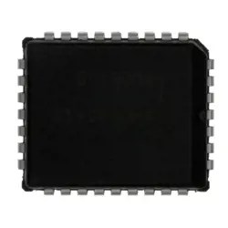
Bilder sind nur zur Referenz
LTC1154CS8
IC GATE DRVR HIGH-SIDE 8SOIC
- Hersteller
- Fr. Teil #LTC1154CS8
- Paket
- Datenblatt LTC1154CS8 DataSheet
- Auf Lager6369
100% Original und Neu
24 Stunden bereit zum Versand
365 Tage Garantie
RFQ & Erhalten Sie mehr Rabatte
Spezifikationen
| Part Status | Obsolete |
| DigiKey Programmable | Not Verified |
| Driven Configuration | High-Side |
| Channel Type | Single |
| Number of Drivers | 1 |
| Gate Type | MOSFET (N-Channel) |
| Voltage - Supply | 4.5V ~ 18V |
| Logic Voltage - VIL, VIH | 0.8V, 2V |
| Input Type | Non-Inverting |
| Operating Temperature | 0°C ~ 70°C (TA) |
| Mounting Type | Surface Mount |
| Package / Case | 8-SOIC (0.154", 3.90mm Width) |
| Supplier Device Package | 8-SO |
| Base Product Number | LTC1154 |
Übersicht
Description
Key features include a built-in hysteresis for noise immunity, a wide input common-mode voltage range, and an output that can drive TTL and CMOS logic levels. Its low power consumption, typically around 60 µA per comparator, enhances efficiency in low-power applications. The device is available in an 8-pin SOIC package, making it compact and easy to integrate into existing designs. The LTC1154 is ideal for applications such as voltage level detection, window comparators, and signal conditioning in various electronic systems.
Features
1. Low Offset Voltage: Typically around 200 µV, ensuring accurate comparisons.
2. Wide Supply Voltage Range: Operates from a single supply of 3V to 36V or dual supplies of ±1.5V to ±18V.
3. High Speed: Fast response time with a propagation delay of 30 ns, suitable for high-speed applications.
4. Low Power Consumption: Consumes only 75 µA maximum, making it energy-efficient.
5. Open-Collector Output: Allows for wired-AND configurations in multi-device applications.
6. Hysteresis: Built-in hysteresis for improved noise immunity and stability.
7. Temperature Range: Operates over a wide temperature range from -40°C to +85°C.
These features make the LTC1154CS8 ideal for voltage-level detection, analog-to-digital conversion, and signal conditioning applications.
Package
Pinout
1. Pin 1 (IN+): Positive input of Comparator A.
2. Pin 2 (IN-): Negative input of Comparator A.
3. Pin 3 (OUT): Output of Comparator A.
4. Pin 4 (GND): Ground connection.
5. Pin 5 (OUTB): Output of Comparator B.
6. Pin 6 (IN-B+): Positive input of Comparator B.
7. Pin 7 (IN-B-): Negative input of Comparator B.
8. Pin 8 (V+): Supply voltage (positive power supply).
The LTC1154CS8 operates on a wide supply voltage range and is designed for applications requiring precise voltage comparison.
Manufacturer
Application
Equivalent
Versand
VersandmethodenWir
bieten Sie globale Versanddienstleistungen durch DHL, FedEx, TNT, UPS oder einen anderen Spediteur Ihrer Wahl.
Versandgebührenreferenz (DHL/FedEx):
DHL: Versandkosten reichen von $25-$45 (0.5kg), mit einer geschätzten Lieferzeit von 2-5 Werktagen.
von FedEx: Versandkosten reichen von $25-$40 (0.5kg), mit einer geschätzten Lieferzeit von 3-7 Werktagen.
UPS: Versandkosten reichen von $25-$45 (0.5kg), mit einer geschätzten Lieferzeit von 3-7 Werktagen.
TNT: Versandkosten reichen von $25-$65 (0.5kg), mit einer geschätzten Lieferzeit von 3-7 Werktagen.
EMS: Versandkosten reichen von $30-$50 (0.5kg), mit einer geschätzten Lieferzeit von 7-15 Werktagen.
Registrierte Luftpost: Versandkosten sind $ 2- $ 4 (0,1 kg), mit einer geschätzten Lieferzeit von 5-20 Werktagen.
Zahlungen
Payment Methods
Die Zahlungsfrist ist 100% Prepaid.
Derzeit akzeptieren wir nur die folgenden Zahlungsmethoden:
1. PayPal
2. Kredit- / Debitkarte
3. Überweisung
Ähnliche
-
![MX25V1635FZNI]() MX25V1635FZNI
MX25V1635FZNI
Macronix
-
![MX66U1G45GXDI00]() MX66U1G45GXDI00
MX66U1G45GXDI00
Macronix
-
![MX25V4035FZUI]() MX25V4035FZUI
MX25V4035FZUI
Macronix
-
![MX25V16066M1I02]() MX25V16066M1I02
MX25V16066M1I02
Macronix
-
![MX25V16066M2I02]() MX25V16066M2I02
MX25V16066M2I02
Macronix
-
![MX25L8035EM2I-10G]() MX25L8035EM2I-10G
MX25L8035EM2I-10G
Macronix
-
![MX25L25673GMI-10G]() MX25L25673GMI-10G
MX25L25673GMI-10G
Macronix
-
![MX25U25643GZNI00]() MX25U25643GZNI00
MX25U25643GZNI00
Macronix
-
![MX25V1635FM2I]() MX25V1635FM2I
MX25V1635FM2I
Macronix
-
![MX25L6433FM2I-08G]() MX25L6433FM2I-08G
MX25L6433FM2I-08G
Macronix
-
![MX29F040CQI-70G]() MX29F040CQI-70G
MX29F040CQI-70G
Macronix
-
![MX30LF4G18AC-TI]() MX30LF4G18AC-TI
MX30LF4G18AC-TI
Macronix