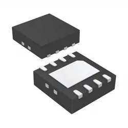
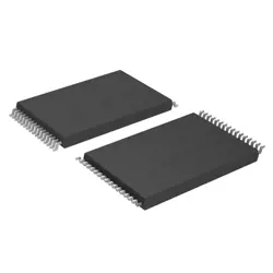
Bilder sind nur zur Referenz
M12L16161A-7TG2Q
- Hersteller
- Fr. Teil #M12L16161A-7TG2Q
- Paket
- Datenblatt M12L16161A-7TG2Q DataSheet
- Auf Lager28839
100% Original und Neu
24 Stunden bereit zum Versand
365 Tage Garantie
RFQ & Erhalten Sie mehr Rabatte
Spezifikationen
| Manufacturer | ESMT(Elite Semicon Memory Tech) |
| Package | TSOP-50-10.0mm |
Übersicht
Description
Key features include fast access times, often around 70 ns, and support for various operating modes, including burst read/write operations, which optimize data throughput. The chip is suitable for applications in consumer electronics, telecommunications, and automotive systems where high-speed data access is required.
The "TG" in its part number signifies a specific package type, and "Q" indicates that it is a lead-free version, adhering to environmental standards such as RoHS. Overall, the M12L16161A-7TG2Q is designed to provide reliable performance in memory-intensive applications while minimizing power consumption.
Features
1. Memory Configuration: 16 Megabit (2M x 8) organization, allowing efficient data storage.
2. Access Speed: Fast access time of 7 ns, suitable for high-performance applications.
3. Operating Voltage: Typically operates at 3.3V, ensuring compatibility with modern low-voltage systems.
4. Refresh: Supports both RAS (Row Address Strobe) and CAS (Column Address Strobe) refreshing methods to maintain data integrity.
5. Packaged in TSOP: Available in a Thin Small Outline Package (TSOP), which provides a compact form factor ideal for space-constrained applications.
6. Compatibility: Compatible with standard DRAM interfaces, making it easy to integrate into various electronic designs.
7. Low Power Consumption: Designed for efficient power usage, making it suitable for battery-operated devices.
These features make the M12L16161A-7TG2Q a reliable choice for consumer electronics, networking, and other applications requiring efficient memory solutions.
Package
Pinout
The primary functions of the pins include:
- Data Inputs/Outputs (DQ0-DQ15): These are used for data transfer.
- Address Inputs (A0-A11): These specify the address of the data being accessed.
- Control Inputs (CK, CK#, CE#, WE#, and OE#): These control the operation of the memory, including clock signals and read/write operations.
- Bank Select Inputs (BA0, BA1): These select the bank of memory being accessed.
- Power and Ground Pins (VDD, VSS): These provide power to the chip and ground connection.
This device operates in a synchronous mode and is designed for high-speed applications.
Manufacturer
Application
Equivalent
Versand
VersandmethodenWir
bieten Sie globale Versanddienstleistungen durch DHL, FedEx, TNT, UPS oder einen anderen Spediteur Ihrer Wahl.
Versandgebührenreferenz (DHL/FedEx):
DHL: Versandkosten reichen von $25-$45 (0.5kg), mit einer geschätzten Lieferzeit von 2-5 Werktagen.
von FedEx: Versandkosten reichen von $25-$40 (0.5kg), mit einer geschätzten Lieferzeit von 3-7 Werktagen.
UPS: Versandkosten reichen von $25-$45 (0.5kg), mit einer geschätzten Lieferzeit von 3-7 Werktagen.
TNT: Versandkosten reichen von $25-$65 (0.5kg), mit einer geschätzten Lieferzeit von 3-7 Werktagen.
EMS: Versandkosten reichen von $30-$50 (0.5kg), mit einer geschätzten Lieferzeit von 7-15 Werktagen.
Registrierte Luftpost: Versandkosten sind $ 2- $ 4 (0,1 kg), mit einer geschätzten Lieferzeit von 5-20 Werktagen.
Zahlungen
Payment Methods
Die Zahlungsfrist ist 100% Prepaid.
Derzeit akzeptieren wir nur die folgenden Zahlungsmethoden:
1. PayPal
2. Kredit- / Debitkarte
3. Überweisung
Ähnliche
-
![MX25V1635FZNQ03]() MX25V1635FZNQ03
MX25V1635FZNQ03
Macronix
-
![MX66U1G45GXDI00]() MX66U1G45GXDI00
MX66U1G45GXDI00
Macronix
-
![MX25V16066M1I02]() MX25V16066M1I02
MX25V16066M1I02
Macronix
-
![MX30LF2G28AD-TI]() MX30LF2G28AD-TI
MX30LF2G28AD-TI
Macronix
-
![MX25L25673GMI-08G]() MX25L25673GMI-08G
MX25L25673GMI-08G
Macronix
-
![MX25L25673GMI-10G]() MX25L25673GMI-10G
MX25L25673GMI-10G
Macronix
-
![MX25U25643GZNI00]() MX25U25643GZNI00
MX25U25643GZNI00
Macronix
-
![MX25L12833FZNI-10G]() MX25L12833FZNI-10..
MX25L12833FZNI-10..
Macronix
-
![MX25U25645GXDI00]() MX25U25645GXDI00
MX25U25645GXDI00
Macronix
-
![MX25L12835FZ2I-10G]() MX25L12835FZ2I-10..
MX25L12835FZ2I-10..
Macronix
-
![MX29LV160DTTI-70G]() MX29LV160DTTI-70G
MX29LV160DTTI-70G
Macronix
-
![MX29F040CTI-70G]() MX29F040CTI-70G
MX29F040CTI-70G
Macronix