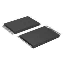
Bilder sind nur zur Referenz
M15T1G1664A
- Hersteller
- Fr. Teil #M15T1G1664A
- Paket
- Datenblatt
- Auf Lager22006
100% Original und Neu
24 Stunden bereit zum Versand
365 Tage Garantie
RFQ & Erhalten Sie mehr Rabatte
Spezifikationen
| Manufacturer | JLCPCB Assembly |
| Package | TFBGA-96_L13.0-W7.5-R16-C6-P0.80-TL |
Übersicht
Description
Designed for high-performance computing applications, the M15T1G1664A offers improved speed and bandwidth compared to earlier DDR SDRAM models. It operates at a voltage of 1.8V, which enhances power efficiency.
Commonly used in various electronic devices such as computers, laptops, and servers, this chip supports various data rates and has multiple functionalities, including burst read/write operations. It adheres to industry standards, making it compatible with a wide range of motherboards and systems.
In summary, the M15T1G1664A is a crucial component in modern computing, facilitating faster data access and processing capabilities.
Features
1. Capacity: Typically provides a density of 1GB, suitable for various applications in consumer electronics and computing.
2. Data Rate: Supports data rates up to 1600 MT/s, enabling efficient data transfer and improved performance.
3. Bus Width: Features a 64-bit data bus, allowing for simultaneous data processing.
4. Voltage: Operates at a low voltage of 1.5V, enhancing power efficiency and reducing heat generation compared to older memory technologies.
5. Package Type: Available in standard packages like TSOPII, facilitating easy integration into PCBs.
6. Compatibility: Designed to be compatible with various DDR3 memory controllers and motherboards.
7. Latency: Offers low latency options, contributing to faster response times in applications.
These features make the M15T1G1664A an ideal choice for laptops, desktops, and embedded systems requiring reliable and efficient memory solutions.
Package
Pinout
Key functions of the pins include:
- Data Pins (DQ): Used for data input and output.
- Address Pins (A): Used for selecting memory locations.
- Control Pins (CK, CK#, CS#, RAS#, CAS#, WE#): Control signals for timing and operation modes.
- VDD and VSS Pins: Power supply and ground connection.
- DQML and DQMH: Byte lane control for data DQ pins.
- ODT (On-Die Termination): Optional termination for signal integrity.
These functions ensure proper operation and data management in memory applications.
Manufacturer
Application
Equivalent
1. MT47H128M8 (Micron)
2. K4T1G164QE (Samsung)
3. Hynix H5TQ1G83AFR (SK Hynix)
4. IS43TR16640D (ISSI)
Always verify specifications and compatibility before substitution.
Versand
VersandmethodenWir
bieten Sie globale Versanddienstleistungen durch DHL, FedEx, TNT, UPS oder einen anderen Spediteur Ihrer Wahl.
Versandgebührenreferenz (DHL/FedEx):
DHL: Versandkosten reichen von $25-$45 (0.5kg), mit einer geschätzten Lieferzeit von 2-5 Werktagen.
von FedEx: Versandkosten reichen von $25-$40 (0.5kg), mit einer geschätzten Lieferzeit von 3-7 Werktagen.
UPS: Versandkosten reichen von $25-$45 (0.5kg), mit einer geschätzten Lieferzeit von 3-7 Werktagen.
TNT: Versandkosten reichen von $25-$65 (0.5kg), mit einer geschätzten Lieferzeit von 3-7 Werktagen.
EMS: Versandkosten reichen von $30-$50 (0.5kg), mit einer geschätzten Lieferzeit von 7-15 Werktagen.
Registrierte Luftpost: Versandkosten sind $ 2- $ 4 (0,1 kg), mit einer geschätzten Lieferzeit von 5-20 Werktagen.
Zahlungen
Payment Methods
Die Zahlungsfrist ist 100% Prepaid.
Derzeit akzeptieren wir nur die folgenden Zahlungsmethoden:
1. PayPal
2. Kredit- / Debitkarte
3. Überweisung
Ähnliche
-
![MX25V2033FM1I]() MX25V2033FM1I
Macronix
-
![MX25V16066M2I02]() MX25V16066M2I02
Macronix
-
![MX30LF2G28AD-TI]() MX30LF2G28AD-TI
Macronix
-
![MX25U51279GXDR00]() MX25U51279GXDR00
Macronix
-
![MX25U3232FZBI02]() MX25U3232FZBI02
Macronix
-
![MX25L12833FM2I-10G]() MX25L12833FM2I-10..
Macronix
-
![MX25L12833FZNI-10G]() MX25L12833FZNI-10..
Macronix
-
![MX25L12835FZ2I-10G]() MX25L12835FZ2I-10..
Macronix
-
![MX29LV160DTTI-70G]() MX29LV160DTTI-70G
Macronix
-
![MX29F040CTI-70G]() MX29F040CTI-70G
Macronix
-
![MX30LF4G18AC-TI]() MX30LF4G18AC-TI
Macronix
-
![MX25R4035FM1IL0]() MX25R4035FM1IL0
Macronix