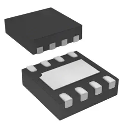
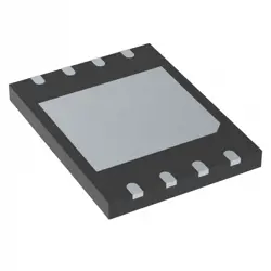
Bilder sind nur zur Referenz
M25PE20-VMN6TP
EEPROM SERIAL PAGE ERASE FLASH 2 Mbit Datas
- Hersteller
- Fr. Teil #M25PE20-VMN6TP
- Paket
- Datenblatt
- Auf Lager9604
100% Original und Neu
24 Stunden bereit zum Versand
365 Tage Garantie
RFQ & Erhalten Sie mehr Rabatte
Spezifikationen
| Packaging | Cut Tape |
| Standard Pack Qty | 2500 |
Übersicht
Description
Key features include:
- Memory Architecture: It typically consists of multiple pages for efficient read/write operations.
- Operating Voltage: The device operates within a specific voltage range, typically around 2.7V to 3.6V.
- Data Retention: It ensures data retention for a specified period, often over 20 years, under normal conditions.
- Program/Erase Cycles: The lifespan of the memory is defined by the number of program/erase cycles, usually around 10,000 to 100,000 cycles.
Overall, the M25PE20-VMN6TP is ideal for applications needing reliable and fast access to stored data.
Features
1. Memory Organization: 256K x 8 bit, ideal for various data storage applications.
2. Serial Peripheral Interface (SPI): Supports high-speed SPI communication, enabling faster data transfer rates.
3. Voltage Range: Operates between 2.5V and 5.5V, making it suitable for various electronic designs.
4. Temperature Range: Available in industrial temperature range options, ensuring reliability in harsh environments.
5. Endurance: Typically supports up to 1 million write/erase cycles, suitable for applications requiring frequent updates.
6. Data Retention: Offers a data retention period of up to 100 years, ensuring long-term reliability.
7. Low Power Consumption: Designed for low power operation, enhancing energy efficiency in battery-powered devices.
8. Multiple Chip Selects: Allows multiple devices to be connected on the same bus, simplifying system design.
This combination of features makes the M25PE20-VMN6TP a robust choice for applications in consumer electronics, automotive, and industrial sectors.
Package
Pinout
Pin Functions:
1. Pin 1 (SCK) - Serial Clock: Input for the clock signal.
2. Pin 2 (SI) - Serial Input: Data input pin for commands and data.
3. Pin 3 (SO) - Serial Output: Data output pin for reading data.
4. Pin 4 (WP) - Write Protect: Input pin to protect memory from accidental writes.
5. Pin 5 (CS) - Chip Select: Active low signal that enables the device.
6. Pin 6 (VSS) - Ground: Connection to the device ground.
7. Pin 7 (VCC) - Supply Voltage: Power supply pin.
8. Pin 8 (HOLD) - Hold: Input pin to pause the operation without losing data.
This device is widely used in embedded systems for non-volatile memory applications.
Manufacturer
Application
Equivalent
Versand
VersandmethodenWir
bieten Sie globale Versanddienstleistungen durch DHL, FedEx, TNT, UPS oder einen anderen Spediteur Ihrer Wahl.
Versandgebührenreferenz (DHL/FedEx):
DHL: Versandkosten reichen von $25-$45 (0.5kg), mit einer geschätzten Lieferzeit von 2-5 Werktagen.
von FedEx: Versandkosten reichen von $25-$40 (0.5kg), mit einer geschätzten Lieferzeit von 3-7 Werktagen.
UPS: Versandkosten reichen von $25-$45 (0.5kg), mit einer geschätzten Lieferzeit von 3-7 Werktagen.
TNT: Versandkosten reichen von $25-$65 (0.5kg), mit einer geschätzten Lieferzeit von 3-7 Werktagen.
EMS: Versandkosten reichen von $30-$50 (0.5kg), mit einer geschätzten Lieferzeit von 7-15 Werktagen.
Registrierte Luftpost: Versandkosten sind $ 2- $ 4 (0,1 kg), mit einer geschätzten Lieferzeit von 5-20 Werktagen.
Zahlungen
Payment Methods
Die Zahlungsfrist ist 100% Prepaid.
Derzeit akzeptieren wir nur die folgenden Zahlungsmethoden:
1. PayPal
2. Kredit- / Debitkarte
3. Überweisung
Ähnliche
-
![MX25V5126FM1I]() MX25V5126FM1I
Macronix
-
![MX25V4035FZUI]() MX25V4035FZUI
Macronix
-
![MX25V2033FM1I]() MX25V2033FM1I
Macronix
-
![MX25R3235FZNIL0]() MX25R3235FZNIL0
Macronix
-
![MX30LF2G28AD-TI]() MX30LF2G28AD-TI
Macronix
-
![MX25R6435FBDIL0]() MX25R6435FBDIL0
Macronix
-
![MX25U51279GXDR00]() MX25U51279GXDR00
Macronix
-
![MX25L2006EM1I-12G]() MX25L2006EM1I-12G
Macronix
-
![MX25R1635FZUIH0]() MX25R1635FZUIH0
Macronix
-
![MX25V1635FM2I]() MX25V1635FM2I
Macronix
-
![MX25U3232FZBI02]() MX25U3232FZBI02
Macronix
-
![MX25L12833FZ2I-10G]() MX25L12833FZ2I-10..
Macronix