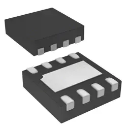
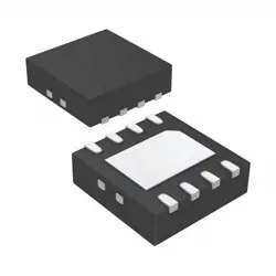
Bilder sind nur zur Referenz
M27C801-100F1
IC EPROM 8MBIT PARALLEL 32CDIP
- Hersteller
- Fr. Teil #M27C801-100F1
- Paket FDIP-32W
- Datenblatt
- Auf Lager2315
100% Original und Neu
24 Stunden bereit zum Versand
365 Tage Garantie
RFQ & Erhalten Sie mehr Rabatte
Spezifikationen
| Package | Tube |
| ProductStatus | Obsolete |
| MemoryType | Non-Volatile |
| MemoryFormat | EPROM |
| Technology | EPROM - UV |
| MemorySize | 8Mb (1M x 8) |
| MemoryInterface | Parallel |
| AccessTime | 100 ns |
| Voltage-Supply | 4.5V ~ 5.5V |
| OperatingTemperature | 0°C ~ 70°C (TA) |
| MountingType | Through Hole |
| Package/Case | 32-CDIP (0.600, 15.24mm) Window |
Übersicht
Description
This chip operates in a dual in-line package (DIP) format, making it suitable for a variety of electronic applications, including embedded systems, automotive, and telecommunications. The M27C801-100F1 allows for electrical erasure, which enables users to rewrite and update the stored data, providing flexibility in programming.
It features a parallel interface for data input and output, supporting a wide voltage range for programming and reading operations. The chip is particularly valuable in environments where frequent updates to firmware or configuration data are necessary, combining reliability with ease of use.
Features
1. Memory Capacity: 8 Mbit (1 MB), organized as 1M x 8 bits.
2. Voltage Supply: Operates at a standard voltage of 5V.
3. Access Time: 100 ns, allowing for fast data retrieval.
4. Package Type: Typically available in a 32-pin DIP (Dual In-line Package) configuration.
5. UV Erasable: Can be erased using ultraviolet light, allowing for reprogramming.
6. Programmability: Supports byte-wise programming, enhancing flexibility in memory management.
7. Data Retention: Offers long-term data retention, typically exceeding 10 years.
8. Compatibility: Compatible with various microprocessor systems that require non-volatile memory.
This device is commonly used in applications such as firmware storage, code development, and embedded systems where reprogramming is necessary.
Package
Pinout
The pin functions are as follows:
1. Address Pins (A0-A19): 20 pins (A0 to A19) for addressing the memory locations.
2. Data Pins (D0-D7): 8 data pins (D0 to D7) for data input/output.
3. Chip Enable (CE): Activates the memory chip for read or write operations.
4. Output Enable (OE): Controls the output data; when active, it allows data to be output.
5. Program Enable (PE): Used for programming the device.
6. Reset (RESET): Resets the internal state of the device.
7. VCC: Power supply pin.
8. VSS: Ground reference pin.
This configuration allows the M27C801-100F1 to read and program data efficiently for a variety of applications.
Manufacturer
Application
Equivalent
Versand
VersandmethodenWir
bieten Sie globale Versanddienstleistungen durch DHL, FedEx, TNT, UPS oder einen anderen Spediteur Ihrer Wahl.
Versandgebührenreferenz (DHL/FedEx):
DHL: Versandkosten reichen von $25-$45 (0.5kg), mit einer geschätzten Lieferzeit von 2-5 Werktagen.
von FedEx: Versandkosten reichen von $25-$40 (0.5kg), mit einer geschätzten Lieferzeit von 3-7 Werktagen.
UPS: Versandkosten reichen von $25-$45 (0.5kg), mit einer geschätzten Lieferzeit von 3-7 Werktagen.
TNT: Versandkosten reichen von $25-$65 (0.5kg), mit einer geschätzten Lieferzeit von 3-7 Werktagen.
EMS: Versandkosten reichen von $30-$50 (0.5kg), mit einer geschätzten Lieferzeit von 7-15 Werktagen.
Registrierte Luftpost: Versandkosten sind $ 2- $ 4 (0,1 kg), mit einer geschätzten Lieferzeit von 5-20 Werktagen.
Zahlungen
Payment Methods
Die Zahlungsfrist ist 100% Prepaid.
Derzeit akzeptieren wir nur die folgenden Zahlungsmethoden:
1. PayPal
2. Kredit- / Debitkarte
3. Überweisung
Ähnliche
-
![MX25R8035FM1IL0]() MX25R8035FM1IL0
MX25R8035FM1IL0
Macronix
-
![MX25V1635FZNI]() MX25V1635FZNI
MX25V1635FZNI
Macronix
-
![MX29F400CBTI-70G]() MX29F400CBTI-70G
MX29F400CBTI-70G
Macronix
-
![MX25V4035FZUI]() MX25V4035FZUI
MX25V4035FZUI
Macronix
-
![MX25V2033FM1I]() MX25V2033FM1I
MX25V2033FM1I
Macronix
-
![MX25V16066M2I02]() MX25V16066M2I02
MX25V16066M2I02
Macronix
-
![MX30LF2G28AD-TI]() MX30LF2G28AD-TI
MX30LF2G28AD-TI
Macronix
-
![MX25L8035EM2I-10G]() MX25L8035EM2I-10G
MX25L8035EM2I-10G
Macronix
-
![MX25L25673GMI-10G]() MX25L25673GMI-10G
MX25L25673GMI-10G
Macronix
-
![MX25R1635FZUIH0]() MX25R1635FZUIH0
MX25R1635FZUIH0
Macronix
-
![MX25L6433FM2I-08G]() MX25L6433FM2I-08G
MX25L6433FM2I-08G
Macronix
-
![MX25L12833FZNI-10G]() MX25L12833FZNI-10..
MX25L12833FZNI-10..
Macronix