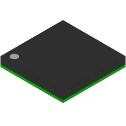
Bilder sind nur zur Referenz
MT25QU02GCBB8E12-0AUT
IC FLASH 2GBIT SPI 24TPBGA
- Hersteller
- Fr. Teil #MT25QU02GCBB8E12-0AUT
- Paket
- Datenblatt
- Auf Lager6479
100% Original und Neu
24 Stunden bereit zum Versand
365 Tage Garantie
RFQ & Erhalten Sie mehr Rabatte
Spezifikationen
| Part Status | Active |
| Base Product Number | MT25QU02 |
| DigiKey Programmable | Not Verified |
| Memory Type | Non-Volatile |
| Memory Format | FLASH |
| Technology | FLASH - NOR |
| Memory Size | 2Gbit |
| Memory Organization | 256M x 8 |
| Memory Interface | SPI - Quad I/O |
| Clock Frequency | 166 MHz |
| Write Cycle Time - Word, Page | 1.8ms |
| Voltage - Supply | 1.7V ~ 2V |
| Operating Temperature | -40°C ~ 125°C (TA) |
| Mounting Type | Surface Mount |
| Package | 24-TBGA |
| Supplier Device Package | 24-T-PBGA (6x8) |
| Packaging | Tray |
| Grade | Automotive |
| Qualification | AEC-Q100 |
Übersicht
Description
Key features include:
- Voltage range: Typically operates at 1.8V for power efficiency.
- Memory organization: It supports various memory configurations and is capable of executing code in place (XIP).
- Enhanced performance: The QSPI interface enables simultaneous read/write operations, significantly improving performance.
- Reliability: It includes advanced error correction and wear leveling mechanisms to enhance data integrity and longevity.
This device is suitable for firmware storage, boot applications, and data logging, making it a versatile choice for modern electronic designs.
Features
Key features include:
- Density: 2Gb (256MB)
- Interface: SPI (Single, Dual, Quad)
- Voltage: Operates at 1.8V
- Read Speed: Up to 104 MHz in Quad SPI mode
- Programming: Supports page programming for efficiency
- Endurance: Typically provides over 100,000 program/erase cycles
- Data Retention: Retains data for up to 20 years at 85°C
- Package: Available in a compact 8-lead SOIC or WSON package
This device is ideal for applications in automotive, industrial, and consumer electronics, where reliable non-volatile storage is essential.
Package
Pinout
Pin Functions:
1. GND: Ground connection.
2. VCC: Supply voltage (typically 2.7V to 3.6V).
3. SCK: Serial clock input.
4. CS#: Chip select (active low).
5. IO0 to IO3: Data input/output lines for serial communication (up to quad I/O).
6. RESET#: Reset input (active low).
7. WP#: Write protect (active low).
8. HOLD#: Hold input (active low).
This configuration allows for high-speed, flexible data storage and retrieval, suitable for various applications in embedded systems.
Manufacturer
Application
Equivalent
Versand
VersandmethodenWir
bieten Sie globale Versanddienstleistungen durch DHL, FedEx, TNT, UPS oder einen anderen Spediteur Ihrer Wahl.
Versandgebührenreferenz (DHL/FedEx):
DHL: Versandkosten reichen von $25-$45 (0.5kg), mit einer geschätzten Lieferzeit von 2-5 Werktagen.
von FedEx: Versandkosten reichen von $25-$40 (0.5kg), mit einer geschätzten Lieferzeit von 3-7 Werktagen.
UPS: Versandkosten reichen von $25-$45 (0.5kg), mit einer geschätzten Lieferzeit von 3-7 Werktagen.
TNT: Versandkosten reichen von $25-$65 (0.5kg), mit einer geschätzten Lieferzeit von 3-7 Werktagen.
EMS: Versandkosten reichen von $30-$50 (0.5kg), mit einer geschätzten Lieferzeit von 7-15 Werktagen.
Registrierte Luftpost: Versandkosten sind $ 2- $ 4 (0,1 kg), mit einer geschätzten Lieferzeit von 5-20 Werktagen.
Zahlungen
Payment Methods
Die Zahlungsfrist ist 100% Prepaid.
Derzeit akzeptieren wir nur die folgenden Zahlungsmethoden:
1. PayPal
2. Kredit- / Debitkarte
3. Überweisung
Ähnliche
-
![MX25L3233FZBI-08Q]() MX25L3233FZBI-08Q
Macronix
-
![MX25V1635FZNQ03]() MX25V1635FZNQ03
Macronix
-
![MX25V5126FM1I]() MX25V5126FM1I
Macronix
-
![MX30LF2G28AD-TI]() MX30LF2G28AD-TI
Macronix
-
![MX25L25673GMI-10G]() MX25L25673GMI-10G
Macronix
-
![MX29GL512FHXFI-11G]() MX29GL512FHXFI-11..
Macronix
-
![MX25L2006EM1I-12G]() MX25L2006EM1I-12G
Macronix
-
![MX25U3232FZBI02]() MX25U3232FZBI02
Macronix
-
![MX25L12833FM2I-10G]() MX25L12833FM2I-10..
Macronix
-
![MX25L12833FZ2I-10G]() MX25L12833FZ2I-10..
Macronix
-
![MX25L12833FZNI-10G]() MX25L12833FZNI-10..
Macronix
-
![MX25U25645GXDI00]() MX25U25645GXDI00
Macronix