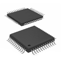
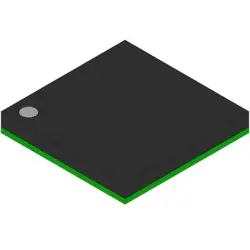
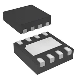
Bilder sind nur zur Referenz
MT40A512M16JY-083E IT:B
DRAM DDR4 8G 512MX16 FBGA
- Hersteller
- Fr. Teil #MT40A512M16JY-083E IT:B
- Paket
- Datenblatt MT40A512M16JY-083E IT:B DataSheet
- Auf Lager22218
100% Original und Neu
24 Stunden bereit zum Versand
365 Tage Garantie
RFQ & Erhalten Sie mehr Rabatte
Spezifikationen
| Packaging | Tray |
| Standard Pack Qty | 1368 |
Übersicht
Description
Key features include:
- Speed Grade: Operates at a data rate of 2400 MT/s (million transfers per second).
- Voltage: Typically operates at a voltage of 1.2V, which helps reduce power consumption compared to previous DDR generations.
- Configuration: x16 configuration, suitable for dual in-line memory modules (DIMMs).
- IT:B: Indicates it is part of a specific industrial temperature grade, suitable for harsher environments.
This chip is ideal for applications requiring fast data access, low latency, and reliability in various operating conditions.
Features
1. Capacity: 8GB (512 Meg x 16 bits).
2. Speed: Operates at a data rate of 2400 MT/s.
3. Organization: 512 Meg x 16 configuration allows for efficient data handling.
4. Die Density: Utilizes a 16-bit wide I/O to enhance bandwidth.
5. Voltage: Operates at a low voltage of 1.2V, improving power efficiency.
6. Package Type: Available in a 96-ball FBGA package, facilitating compact designs.
7. Temperature Range: Designed for industrial applications, rated for -40°C to +95°C.
8. Error Correction: Supports ECC (Error Correction Code) for improved reliability.
9. Compatibility: Suitable for various applications including networking, data centers, and high-performance computing.
This module is ideal for environments requiring robust performance and stability under varying temperatures.
Package
Pinout
Key functions of the pins include:
- Data Pins (DQ): These are used for data input and output.
- Address Pins (A): They are utilized to select memory locations.
- Control Pins (CK, CK#, CS, WE, RAS, CAS, etc.): These control signals manage the operation of the memory, including read/write commands and timing.
- Power and Ground Pins (VDD, VSS): These provide the necessary power supply and ground reference for the chip.
This memory component is designed for high-performance applications in computing and networking, providing efficient data handling.
Manufacturer
Application
Equivalent
1. Hynix H5TQ2G83AFR
2. Samsung K4B2G1646C
3. Micron MT41K256M16HA
4. Nanya NT5CB256M16FP-DI
Ensure to check specifications like timings, voltage, and density for compatibility.
Versand
VersandmethodenWir
bieten Sie globale Versanddienstleistungen durch DHL, FedEx, TNT, UPS oder einen anderen Spediteur Ihrer Wahl.
Versandgebührenreferenz (DHL/FedEx):
DHL: Versandkosten reichen von $25-$45 (0.5kg), mit einer geschätzten Lieferzeit von 2-5 Werktagen.
von FedEx: Versandkosten reichen von $25-$40 (0.5kg), mit einer geschätzten Lieferzeit von 3-7 Werktagen.
UPS: Versandkosten reichen von $25-$45 (0.5kg), mit einer geschätzten Lieferzeit von 3-7 Werktagen.
TNT: Versandkosten reichen von $25-$65 (0.5kg), mit einer geschätzten Lieferzeit von 3-7 Werktagen.
EMS: Versandkosten reichen von $30-$50 (0.5kg), mit einer geschätzten Lieferzeit von 7-15 Werktagen.
Registrierte Luftpost: Versandkosten sind $ 2- $ 4 (0,1 kg), mit einer geschätzten Lieferzeit von 5-20 Werktagen.
Zahlungen
Payment Methods
Die Zahlungsfrist ist 100% Prepaid.
Derzeit akzeptieren wir nur die folgenden Zahlungsmethoden:
1. PayPal
2. Kredit- / Debitkarte
3. Überweisung
Ähnliche
-
![MX25V1635FZNI]() MX25V1635FZNI
Macronix
-
![MX29F400CBTI-70G]() MX29F400CBTI-70G
Macronix
-
![MX25V2033FM1I]() MX25V2033FM1I
Macronix
-
![MX25V16066M1I02]() MX25V16066M1I02
Macronix
-
![MX25V16066M2I02]() MX25V16066M2I02
Macronix
-
![MX25R6435FBDIL0]() MX25R6435FBDIL0
Macronix
-
![MX25L25673GMI-08G]() MX25L25673GMI-08G
Macronix
-
![MX29GL512FHXFI-11G]() MX29GL512FHXFI-11..
Macronix
-
![MX25L2006EM1I-12G]() MX25L2006EM1I-12G
Macronix
-
![MX25R1635FZUIH0]() MX25R1635FZUIH0
Macronix
-
![MX25V1635FM2I]() MX25V1635FM2I
Macronix
-
![MX25U6435FM2I-10G]() MX25U6435FM2I-10G
Macronix