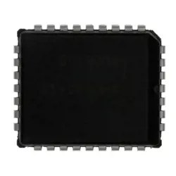
Bilder sind nur zur Referenz
MT41K256M16TW-125:P
IC DRAM 4GBIT PARALLEL 96FBGA
- Hersteller
- Fr. Teil #MT41K256M16TW-125:P
- Paket
- Datenblatt
- Auf Lager2141
100% Original und Neu
24 Stunden bereit zum Versand
365 Tage Garantie
RFQ & Erhalten Sie mehr Rabatte
Spezifikationen
| Part Status | Obsolete |
| Base Product Number | MT41K256M16 |
| DigiKey Programmable | Not Verified |
| Memory Type | Volatile |
| Memory Format | DRAM |
| Technology | SDRAM - DDR3L |
| Memory Size | 4Gbit |
| Memory Organization | 256M x 16 |
| Memory Interface | Parallel |
| Clock Frequency | 800 MHz |
| Voltage - Supply | 1.283V ~ 1.45V |
| Operating Temperature | 0°C ~ 95°C (TC) |
| Mounting Type | Surface Mount |
| Package | 96-TFBGA |
| Supplier Device Package | 96-FBGA (8x14) |
| Packaging | Tray |
| Access Time | 20 ns |
Übersicht
Description
Key features include low power consumption, making it suitable for mobile and high-performance computing applications. The chip operates at a voltage of 1.5V, offering improved energy efficiency compared to older DRAM technologies. The MT41K256M16TW-125:P is commonly used in various devices, including laptops, desktops, and servers, providing reliable and high-speed memory performance for demanding applications. Its compact design and adherence to industry standards allow for easy integration into various electronic systems.
Features
This memory chip utilizes a 78-ball FBGA package and is designed for use in various applications, including desktops, laptops, and servers. It includes built-in self-test (BIST) capabilities for improved reliability and performance. The MT41K256M16TW-125:P also features advanced power-saving modes, enhancing energy efficiency. It is RoHS compliant and suitable for high-performance computing environments, making it a reliable choice for modern memory solutions.
Package
Pinout
Key functions of the pins include:
- Data Pins (DQ): 16 data pins for read/write operations.
- Address Pins (A): Used to select memory locations.
- Control Pins: Includes signals like Chip Select (CS), Write Enable (WE), and Read Enable (RE) for controlling memory operations.
- Clock Pins (CK, CK#): Differential clock inputs for timing.
- Power Supply Pins: Supply voltage (VDD) and ground (VSS).
- Mode Register Set (MRS) Pins: For configuring the memory's operational parameters.
The chip supports various features such as on-die termination (ODT) and is compliant with the DDR3 SDRAM standard, making it suitable for a wide range of applications in consumer electronics and computing devices.
Manufacturer
Application
Equivalent
1. Hynix H5TQ4G83CFR-PBA
2. Samsung K4B4G1646F-BCK0
3. Micron MT41K256M16HA-125
4. Nanya NT5CB256M16DP-DI
Always verify compatibility and specifications before substitution.
Versand
VersandmethodenWir
bieten Sie globale Versanddienstleistungen durch DHL, FedEx, TNT, UPS oder einen anderen Spediteur Ihrer Wahl.
Versandgebührenreferenz (DHL/FedEx):
DHL: Versandkosten reichen von $25-$45 (0.5kg), mit einer geschätzten Lieferzeit von 2-5 Werktagen.
von FedEx: Versandkosten reichen von $25-$40 (0.5kg), mit einer geschätzten Lieferzeit von 3-7 Werktagen.
UPS: Versandkosten reichen von $25-$45 (0.5kg), mit einer geschätzten Lieferzeit von 3-7 Werktagen.
TNT: Versandkosten reichen von $25-$65 (0.5kg), mit einer geschätzten Lieferzeit von 3-7 Werktagen.
EMS: Versandkosten reichen von $30-$50 (0.5kg), mit einer geschätzten Lieferzeit von 7-15 Werktagen.
Registrierte Luftpost: Versandkosten sind $ 2- $ 4 (0,1 kg), mit einer geschätzten Lieferzeit von 5-20 Werktagen.
Zahlungen
Payment Methods
Die Zahlungsfrist ist 100% Prepaid.
Derzeit akzeptieren wir nur die folgenden Zahlungsmethoden:
1. PayPal
2. Kredit- / Debitkarte
3. Überweisung
Ähnliche
-
![MX25R8035FM1IL0]() MX25R8035FM1IL0
MX25R8035FM1IL0
Macronix
-
![MX25L3233FZBI-08Q]() MX25L3233FZBI-08Q
MX25L3233FZBI-08Q
Macronix
-
![MX25V1635FZNQ03]() MX25V1635FZNQ03
MX25V1635FZNQ03
Macronix
-
![MX25V5126FM1I]() MX25V5126FM1I
MX25V5126FM1I
Macronix
-
![MX25V16066M2I02]() MX25V16066M2I02
MX25V16066M2I02
Macronix
-
![MX25L8035EM2I-10G]() MX25L8035EM2I-10G
MX25L8035EM2I-10G
Macronix
-
![MX29GL512FHXFI-11G]() MX29GL512FHXFI-11..
MX29GL512FHXFI-11..
Macronix
-
![MX25L6433FM2I-08G]() MX25L6433FM2I-08G
MX25L6433FM2I-08G
Macronix
-
![MX25L12833FM2I-10G]() MX25L12833FM2I-10..
MX25L12833FM2I-10..
Macronix
-
![MX25U25645GXDI00]() MX25U25645GXDI00
MX25U25645GXDI00
Macronix
-
![MX25L12835FZ2I-10G]() MX25L12835FZ2I-10..
MX25L12835FZ2I-10..
Macronix
-
![MX29F040CQI-70G]() MX29F040CQI-70G
MX29F040CQI-70G
Macronix