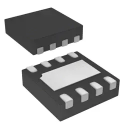
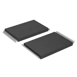
Bilder sind nur zur Referenz
MT48LC8M16A2P-75 IT:G
3V~3.6V 128Mbit 133MHz 54-TSOP II Memory (ICs) RoHS
- Hersteller
- Fr. Teil #MT48LC8M16A2P-75 IT:G
- Paket
- Datenblatt
- Auf Lager10908
100% Original und Neu
24 Stunden bereit zum Versand
365 Tage Garantie
RFQ & Erhalten Sie mehr Rabatte
Spezifikationen
| Packaging | 54-TSOP II |
| Clock Frequency | 133MHz |
| Memory Size | 128Mbit |
| Operating temperature | -40℃~+85℃ |
| Voltage - Supply | 3V~3.6V |
Übersicht
Description
This memory chip operates on a 3.3V power supply and supports various operating modes and configurations, including burst mode operations. It is commonly used in applications such as telecommunications, industrial computing, and automotive systems where reliability and performance are critical.
Overall, the MT48LC8M16A2P-75 IT:G is designed for high-speed data processing needs while maintaining efficiency in power consumption. Its robust performance and durability make it an ideal choice for demanding applications.
Features
1. Type: DDR SDRAM (Double Data Rate Synchronous Dynamic Random Access Memory).
2. Capacity: 128 Megabits (16 Megabytes) per chip, organized as 8M x 16 bits.
3. Speed: Operates at a clock speed of 75 MHz (hence the -75 in the part number).
4. Package: Available in a 54-ball TFBGA (Thin Fine-Pitch Ball Grid Array) package.
5. Voltage: Operates at a low voltage of 3.3V.
6. Access Time: Supports fast access times suitable for various applications.
7. Temperature Range: IT indicates an Industrial temperature range, typically from -40°C to +85°C, making it suitable for harsh environments.
8. Functionality: Ideal for use in applications requiring high-density memory, such as telecommunications, networking, and industrial systems.
This chip is designed for reliable performance and durability in demanding applications.
Package
Pinout
The pin functions include:
1. Address Pins (A0-A12): Used for addressing the memory cells.
2. Data Pins (DQ0-DQ7): 8-bit data input/output pins.
3. Control Pins:
- WE (Write Enable): Activates write operations.
- RE (Read Enable): Activates read operations.
- CS (Chip Select): Enables the chip for operation.
4. Baud Pins (BA0, BA1): Select bank for memory access.
5. VDD/VSS: Power supply and ground connections.
6. DQM (Data Mask): Controls data output during read/write operations.
This chip operates at a maximum clock frequency of 133 MHz with a cycle time of 7.5 ns, suitable for various applications requiring dynamic memory.
Manufacturer
Application
Equivalent
1. Micron MT47H64M16HR-25
2. Hynix H5TQ2G83AFR
3. Nanya NT5TU128M8DA-25
4. Samsung K4T1G164QE-HCB3
Ensure compatibility with specific application requirements before substitution.
Versand
VersandmethodenWir
bieten Sie globale Versanddienstleistungen durch DHL, FedEx, TNT, UPS oder einen anderen Spediteur Ihrer Wahl.
Versandgebührenreferenz (DHL/FedEx):
DHL: Versandkosten reichen von $25-$45 (0.5kg), mit einer geschätzten Lieferzeit von 2-5 Werktagen.
von FedEx: Versandkosten reichen von $25-$40 (0.5kg), mit einer geschätzten Lieferzeit von 3-7 Werktagen.
UPS: Versandkosten reichen von $25-$45 (0.5kg), mit einer geschätzten Lieferzeit von 3-7 Werktagen.
TNT: Versandkosten reichen von $25-$65 (0.5kg), mit einer geschätzten Lieferzeit von 3-7 Werktagen.
EMS: Versandkosten reichen von $30-$50 (0.5kg), mit einer geschätzten Lieferzeit von 7-15 Werktagen.
Registrierte Luftpost: Versandkosten sind $ 2- $ 4 (0,1 kg), mit einer geschätzten Lieferzeit von 5-20 Werktagen.
Zahlungen
Payment Methods
Die Zahlungsfrist ist 100% Prepaid.
Derzeit akzeptieren wir nur die folgenden Zahlungsmethoden:
1. PayPal
2. Kredit- / Debitkarte
3. Überweisung
Ähnliche
-
![MX25R8035FM1IL0]() MX25R8035FM1IL0
MX25R8035FM1IL0
Macronix
-
![MX25L3233FM1I-08Q]() MX25L3233FM1I-08Q
MX25L3233FM1I-08Q
Macronix
-
![MX25V1635FZNQ03]() MX25V1635FZNQ03
MX25V1635FZNQ03
Macronix
-
![MX29F400CBTI-70G]() MX29F400CBTI-70G
MX29F400CBTI-70G
Macronix
-
![MX25V5126FM1I]() MX25V5126FM1I
MX25V5126FM1I
Macronix
-
![MX25R3235FZNIL0]() MX25R3235FZNIL0
MX25R3235FZNIL0
Macronix
-
![MX25L8035EM2I-10G]() MX25L8035EM2I-10G
MX25L8035EM2I-10G
Macronix
-
![MX25R6435FBDIL0]() MX25R6435FBDIL0
MX25R6435FBDIL0
Macronix
-
![MX25R1635FZUIH0]() MX25R1635FZUIH0
MX25R1635FZUIH0
Macronix
-
![MX25U25645GXDI00]() MX25U25645GXDI00
MX25U25645GXDI00
Macronix
-
![MX29LV160DTTI-70G]() MX29LV160DTTI-70G
MX29LV160DTTI-70G
Macronix
-
![MX29F040CTI-70G]() MX29F040CTI-70G
MX29F040CTI-70G
Macronix