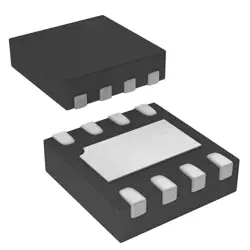
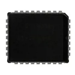
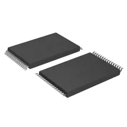
Bilder sind nur zur Referenz
NB3V1104CDTR2G
IC CLK BUFFER 1:4 250MHZ 8TSSOP
- Hersteller
- Fr. Teil #NB3V1104CDTR2G
- Paket
- Datenblatt NB3V1104CDTR2G DataSheet
- Auf Lager9209
100% Original und Neu
24 Stunden bereit zum Versand
365 Tage Garantie
RFQ & Erhalten Sie mehr Rabatte
Spezifikationen
| Part Status | Active |
| Type | Fanout Buffer (Distribution) |
| Number of Circuits | 1 |
| Ratio - Input:Output | 1:4 |
| Differential - Input:Output | No/No |
| Input | LVCMOS |
| Output | LVCMOS |
| Frequency - Max | 250 MHz |
| Voltage - Supply | 1.71V ~ 3.6V |
| Operating Temperature | -40°C ~ 105°C |
| Mounting Type | Surface Mount |
| Package / Case | 8-TSSOP (0.173", 4.40mm Width) |
| Supplier Device Package | 8-TSSOP |
| Base Product Number | NB3V1104 |
Übersicht
Description
Key features include low propagation delay, low jitter, and high output drive capability, enabling reliable signal distribution in high-speed systems. The NB3V1104CDTR2G is available in a compact surface-mount package, enhancing PCB layout flexibility.
Due to its robust performance and versatility, it is commonly used in applications requiring clock distribution, such as microprocessors, FPGAs, and ASICs. Overall, the NB3V1104CDTR2G is an essential component for achieving optimal timing performance in complex digital circuits.
Features
1. Multiple Outputs: It has four clock outputs, enabling the distribution of a single clock signal to multiple devices.
2. Low Jitter: The device provides low output jitter, enhancing signal integrity for high-speed applications.
3. Wide Supply Voltage Range: Operates from a supply voltage of 3.0V to 3.6V, making it adaptable to different system requirements.
4. High Drive Capability: Capable of driving large capacitive loads, ensuring reliable signal transmission over longer distances.
5. Temperature Range: Designed for operation across a commercial temperature range of 0°C to 85°C, suitable for various environments.
6. Small Package Size: Available in a compact SOIC-8 package, which is beneficial for space-constrained applications.
These features make the NB3V1104CDTR2G ideal for applications requiring precise clock distribution and low signal degradation.
Package
Pinout
The key features include:
- Input/Output: It supports four differential input pairs (IN1+, IN1-, IN2+, IN2-, IN3+, IN3-, IN4+, IN4-) with corresponding differential output pairs (OUT1+, OUT1-, OUT2+, OUT2-, OUT3+, OUT3-, OUT4+, OUT4-).
- Voltage Supply: It operates with a supply voltage range of 2.5V to 3.6V.
- Data Rate: Capable of supporting data rates up to 1.5 Gbps.
- Applications: Commonly used in high-speed communication applications, such as video and data transmission systems.
The device is packaged in a small footprint, making it suitable for space-constrained designs.
Manufacturer
Application
Equivalent
Versand
VersandmethodenWir
bieten Sie globale Versanddienstleistungen durch DHL, FedEx, TNT, UPS oder einen anderen Spediteur Ihrer Wahl.
Versandgebührenreferenz (DHL/FedEx):
DHL: Versandkosten reichen von $25-$45 (0.5kg), mit einer geschätzten Lieferzeit von 2-5 Werktagen.
von FedEx: Versandkosten reichen von $25-$40 (0.5kg), mit einer geschätzten Lieferzeit von 3-7 Werktagen.
UPS: Versandkosten reichen von $25-$45 (0.5kg), mit einer geschätzten Lieferzeit von 3-7 Werktagen.
TNT: Versandkosten reichen von $25-$65 (0.5kg), mit einer geschätzten Lieferzeit von 3-7 Werktagen.
EMS: Versandkosten reichen von $30-$50 (0.5kg), mit einer geschätzten Lieferzeit von 7-15 Werktagen.
Registrierte Luftpost: Versandkosten sind $ 2- $ 4 (0,1 kg), mit einer geschätzten Lieferzeit von 5-20 Werktagen.
Zahlungen
Payment Methods
Die Zahlungsfrist ist 100% Prepaid.
Derzeit akzeptieren wir nur die folgenden Zahlungsmethoden:
1. PayPal
2. Kredit- / Debitkarte
3. Überweisung
Ähnliche
-
![MX25L3233FM1I-08Q]() MX25L3233FM1I-08Q
MX25L3233FM1I-08Q
Macronix
-
![MX25V1635FZNQ03]() MX25V1635FZNQ03
MX25V1635FZNQ03
Macronix
-
![MX25V4035FZUI]() MX25V4035FZUI
MX25V4035FZUI
Macronix
-
![MX25V16066M1I02]() MX25V16066M1I02
MX25V16066M1I02
Macronix
-
![MX25L8035EM2I-10G]() MX25L8035EM2I-10G
MX25L8035EM2I-10G
Macronix
-
![MX25U3232FZBI02]() MX25U3232FZBI02
MX25U3232FZBI02
Macronix
-
![MX25L6433FM2I-08G]() MX25L6433FM2I-08G
MX25L6433FM2I-08G
Macronix
-
![MX25U6435FM2I-10G]() MX25U6435FM2I-10G
MX25U6435FM2I-10G
Macronix
-
![MX25L12833FM2I-10G]() MX25L12833FM2I-10..
MX25L12833FM2I-10..
Macronix
-
![MX25L12833FZ2I-10G]() MX25L12833FZ2I-10..
MX25L12833FZ2I-10..
Macronix
-
![MX29F040CQI-70G]() MX29F040CQI-70G
MX29F040CQI-70G
Macronix
-
![MX29F040CTI-70G]() MX29F040CTI-70G
MX29F040CTI-70G
Macronix