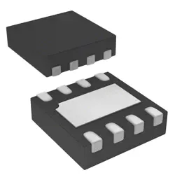
Bilder sind nur zur Referenz
NCP3063DR2G
IC REG BUCK BST ADJ 1.5A 8SOIC
- Hersteller
- Fr. Teil #NCP3063DR2G
- Paket SOIC-8
- Datenblatt
- Auf Lager2738
100% Original und Neu
24 Stunden bereit zum Versand
365 Tage Garantie
RFQ & Erhalten Sie mehr Rabatte
Spezifikationen
| Package | Tape & Reel (TR),Cut Tape (CT) |
| ProductStatus | Active |
| Function | Step-Up, Step-Down |
| OutputConfiguration | Positive or Negative |
| Topology | Buck, Boost |
| OutputType | Adjustable |
| NumberofOutputs | 1 |
| Voltage-Input(Min) | 3V |
| Voltage-Input(Max) | 40V |
| Voltage-Output(Min/Fixed) | 1.25V |
| Voltage-Output(Max) | 40V (Switch) |
| Current-Output | 1.5A (Switch) |
| Frequency-Switching | 150kHz |
| SynchronousRectifier | No |
| OperatingTemperature | 0°C ~ 70°C (TJ) |
| MountingType | Surface Mount |
| Package/Case | 8-SOIC (0.154, 3.90mm Width) |
Übersicht
Description
Key features of the NCP3063DR2G include a switching frequency of 150 kHz, which allows for the use of smaller inductors and capacitors, contributing to a more compact design. The IC also offers an adjustable output voltage, current limiting, and thermal shutdown for protection against overheating. Its high efficiency, typically over 80%, ensures minimal power loss during conversion.
The NCP3063DR2G is available in a standard SOIC-8 (Small Outline Integrated Circuit) package, which is convenient for PCB layouts. Its robust performance and flexibility make it a popular choice for designers looking to implement efficient power management solutions in automotive, industrial, and consumer electronics applications.
Features
Package
Pinout
Here's a brief overview of the pin functions:
1. Pin 1 (Switch Collector - C): Connects to the inductor or transformer.
2. Pin 2 (Emitter - E): Connects to the switching transistor's emitter terminal.
3. Pin 3 (Timing Capacitor - CT): Used to set the oscillator frequency.
4. Pin 4 (Ground - GND): Common ground for the IC.
5. Pin 5 (Comparator Inverting Input - INV): Connects to the feedback loop to regulate output voltage.
6. Pin 6 (VCC): Power supply input for the IC.
7. Pin 7 (Switch Base - B): Drives the base of the internal switching transistor.
8. Pin 8 (Voltage Feedback - VFB): Provides feedback for voltage regulation.
This IC is valued for its flexibility, allowing designers to tailor circuits to specific power conversion needs.
Manufacturer
Application
Equivalent
1. MC34063A - by Texas Instruments
2. LM2576 - by Texas Instruments
3. MC33063 - by STMicroelectronics
4. LM2596 - by Texas Instruments
5. LMR16006 - by Texas Instruments
These alternatives vary in features and specifications, so it's important to compare them according to your specific design requirements.
Versand
VersandmethodenWir
bieten Sie globale Versanddienstleistungen durch DHL, FedEx, TNT, UPS oder einen anderen Spediteur Ihrer Wahl.
Versandgebührenreferenz (DHL/FedEx):
DHL: Versandkosten reichen von $25-$45 (0.5kg), mit einer geschätzten Lieferzeit von 2-5 Werktagen.
von FedEx: Versandkosten reichen von $25-$40 (0.5kg), mit einer geschätzten Lieferzeit von 3-7 Werktagen.
UPS: Versandkosten reichen von $25-$45 (0.5kg), mit einer geschätzten Lieferzeit von 3-7 Werktagen.
TNT: Versandkosten reichen von $25-$65 (0.5kg), mit einer geschätzten Lieferzeit von 3-7 Werktagen.
EMS: Versandkosten reichen von $30-$50 (0.5kg), mit einer geschätzten Lieferzeit von 7-15 Werktagen.
Registrierte Luftpost: Versandkosten sind $ 2- $ 4 (0,1 kg), mit einer geschätzten Lieferzeit von 5-20 Werktagen.
Zahlungen
Payment Methods
Die Zahlungsfrist ist 100% Prepaid.
Derzeit akzeptieren wir nur die folgenden Zahlungsmethoden:
1. PayPal
2. Kredit- / Debitkarte
3. Überweisung
Ähnliche
-
![MX25L3233FM1I-08Q]() MX25L3233FM1I-08Q
MX25L3233FM1I-08Q
Macronix
-
![MX25V1635FZNI]() MX25V1635FZNI
MX25V1635FZNI
Macronix
-
![MX25V4035FZUI]() MX25V4035FZUI
MX25V4035FZUI
Macronix
-
![MX25V2033FM1I]() MX25V2033FM1I
MX25V2033FM1I
Macronix
-
![MX25L25673GMI-08G]() MX25L25673GMI-08G
MX25L25673GMI-08G
Macronix
-
![MX29GL512FHXFI-11G]() MX29GL512FHXFI-11..
MX29GL512FHXFI-11..
Macronix
-
![MX25R1635FZUIH0]() MX25R1635FZUIH0
MX25R1635FZUIH0
Macronix
-
![MX25V1635FM2I]() MX25V1635FM2I
MX25V1635FM2I
Macronix
-
![MX25U6435FM2I-10G]() MX25U6435FM2I-10G
MX25U6435FM2I-10G
Macronix
-
![MX25U25645GXDI00]() MX25U25645GXDI00
MX25U25645GXDI00
Macronix
-
![MX29LV160DTTI-70G]() MX29LV160DTTI-70G
MX29LV160DTTI-70G
Macronix
-
![MX25L25645GXDI-08G]() MX25L25645GXDI-08..
MX25L25645GXDI-08..
Macronix