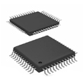
Bilder sind nur zur Referenz
NT5CB128M16JR-FL
2Gbit 1.066GHz DDR3 SDRAM TFBGA-96 Memory (ICs) RoHS
- Hersteller
- Fr. Teil #NT5CB128M16JR-FL
- Paket
- Datenblatt NT5CB128M16JR-FL DataSheet
- Auf Lager15628
100% Original und Neu
24 Stunden bereit zum Versand
365 Tage Garantie
RFQ & Erhalten Sie mehr Rabatte
Spezifikationen
| Packaging | TFBGA-96 |
| Clock Frequency | 1.066GHz |
| Memory Format | DDR3 SDRAM |
| Memory Size | 2Gbit |
| Operating temperature | 0℃~+95℃ |
| Voltage - Supply | 1.425V~1.575V;1.283V~1.45V |
Übersicht
Description
This memory operates at low voltage (1.5V) and supports data rates from 800 to 1600 MT/s (million transfers per second), which enhances overall system performance. Its features include burst mode operation, programmable latency, and on-die termination (ODT), ensuring efficient data handling and power management. The NT5CB128M16JR-FL is commonly used in applications requiring reliable, high-speed memory with lower power consumption, making it a popular choice in modern electronics.
Features
- Density: 1GB capacity with 128M x 16 organization.
- Speed: Compatible with DDR3-1600/1333/1066 speeds.
- Package: Offered in a 78-ball FBGA (Fine Ball Grid Array) package for compact designs.
- Operating Temperature: Typically supports a range from -40°C to 85°C, making it suitable for industrial applications.
- Data Integrity: Supports features like on-die termination (ODT) and is compliant with JEDEC standards for reliability.
- Applications: Ideal for use in consumer electronics, networking, and industrial equipment.
The NT5CB128M16JR-FL is characterized by its efficiency and high bandwidth, meeting the demands of modern computing systems.
Package
Pinout
The primary functions of the pins include:
- Data I/O Pins (DQ): Used for data input and output during read and write operations.
- Address Pins (A): Used to select memory addresses for read and write operations.
- Control Pins (CS, RAS, CAS, WE): Control signals for memory operations.
- Clock Pins (CK, CK#): Provide the clock signal necessary for synchronization.
- Power and Ground Pins (VDD, VSS): Supply power to the chip and ground reference.
This chip is typically used in various applications such as computers, servers, and embedded systems requiring DRAM memory.
Manufacturer
Application
Equivalent
Versand
VersandmethodenWir
bieten Sie globale Versanddienstleistungen durch DHL, FedEx, TNT, UPS oder einen anderen Spediteur Ihrer Wahl.
Versandgebührenreferenz (DHL/FedEx):
DHL: Versandkosten reichen von $25-$45 (0.5kg), mit einer geschätzten Lieferzeit von 2-5 Werktagen.
von FedEx: Versandkosten reichen von $25-$40 (0.5kg), mit einer geschätzten Lieferzeit von 3-7 Werktagen.
UPS: Versandkosten reichen von $25-$45 (0.5kg), mit einer geschätzten Lieferzeit von 3-7 Werktagen.
TNT: Versandkosten reichen von $25-$65 (0.5kg), mit einer geschätzten Lieferzeit von 3-7 Werktagen.
EMS: Versandkosten reichen von $30-$50 (0.5kg), mit einer geschätzten Lieferzeit von 7-15 Werktagen.
Registrierte Luftpost: Versandkosten sind $ 2- $ 4 (0,1 kg), mit einer geschätzten Lieferzeit von 5-20 Werktagen.
Zahlungen
Payment Methods
Die Zahlungsfrist ist 100% Prepaid.
Derzeit akzeptieren wir nur die folgenden Zahlungsmethoden:
1. PayPal
2. Kredit- / Debitkarte
3. Überweisung
Ähnliche
-
![MX25L3233FZBI-08Q]() MX25L3233FZBI-08Q
Macronix
-
![MX66U1G45GXDI00]() MX66U1G45GXDI00
Macronix
-
![MX25V5126FM1I]() MX25V5126FM1I
Macronix
-
![MX25V4035FZUI]() MX25V4035FZUI
Macronix
-
![MX25V2033FM1I]() MX25V2033FM1I
Macronix
-
![MX25V16066M2I02]() MX25V16066M2I02
Macronix
-
![MX30LF2G28AD-TI]() MX30LF2G28AD-TI
Macronix
-
![MX25R6435FBDIL0]() MX25R6435FBDIL0
Macronix
-
![MX25L25673GMI-10G]() MX25L25673GMI-10G
Macronix
-
![MX25U25643GZNI00]() MX25U25643GZNI00
Macronix
-
![MX25L6433FM2I-08G]() MX25L6433FM2I-08G
Macronix
-
![MX25L12833FM2I-10G]() MX25L12833FM2I-10..
Macronix