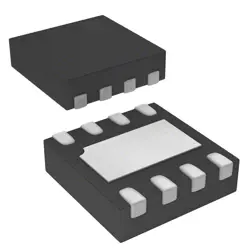
Bilder sind nur zur Referenz
NT6TL128T64BR-G0
- Hersteller
- Fr. Teil #NT6TL128T64BR-G0
- Paket
- Datenblatt
- Auf Lager12848
100% Original und Neu
24 Stunden bereit zum Versand
365 Tage Garantie
RFQ & Erhalten Sie mehr Rabatte
Spezifikationen
| EU RoHS | Compliant |
| ECCN (US) | EAR99 |
| Part Status | Active |
| HTS | 8542.32.00.36 |
| Automotive | Unknown |
| PPAP | Unknown |
| Mounting | Surface Mount |
| Package Height | 0.59(Max) |
| Package Width | 12 |
| Package Length | 12 |
| PCB changed | 216 |
| Standard Package Name | BGA |
| Supplier Package | POP-FBGA |
| Pin Count | 216 |
| Lead Shape | Ball |
Übersicht
Description
This DDR3 SDRAM module operates at a voltage of 1.5V, allowing for lower power consumption compared to its predecessors. It supports a data rate of up to 1600 MT/s (megatransfers per second), enhancing data transfer speeds and overall system performance. The chip is packaged in a standard FBGA (Fine Pitch Ball Grid Array) format, facilitating easy integration into electronic circuits.
Additionally, the NT6TL128T64BR-G0 complies with industry standards, ensuring reliability and compatibility with a wide range of systems. Its features make it an essential component for users looking to enhance their computing experience through improved memory performance.
Features
1. Type: DDR3 SDRAM
2. Capacity: 1 Gigabit (128 Megabytes x 64)
3. Configuration: 128M x 64 bits organization
4. Speed: Operates at a data rate of 1066 MT/s (megatransfers per second)
5. Voltage: 1.5V operating voltage
6. Package: Typically available in a FBGA (Fine Ball Grid Array) package
7. Latency: Offers low latency for improved performance in various applications.
8. Applications: Suitable for use in servers, networking equipment, and other memory-intensive applications.
This module provides improved bandwidth and energy efficiency compared to earlier DDR2 modules, making it a popular choice for modern electronic systems.
Package
Pinout
The primary functions of the pins include data input/output, address, command, control signals, and power connections. Key pin functions include:
- Data Pins (DQ0-DQ63): Used for data transfer.
- Address Pins (A0-A12, BA0-BA2): Used for addressing memory locations.
- Control Pins (CK, CK#, CS#, RAS#, CAS#, WE#): Used for controlling the memory operations.
- Power and Ground Pins (VDD, VSS): Provide power supply and ground connection.
This configuration is suitable for high-performance applications in computers and other electronic devices.
Manufacturer
Application
Equivalent
1. MT6HT12864HY-667
2. Hynix HYMD516646B6D
3. KVR667D2N5/1G (Kingston)
4. M471B5673FH0-CH9 (Samsung)
Always verify compatibility based on specific requirements like timings, voltage, and density before substitution.
Versand
VersandmethodenWir
bieten Sie globale Versanddienstleistungen durch DHL, FedEx, TNT, UPS oder einen anderen Spediteur Ihrer Wahl.
Versandgebührenreferenz (DHL/FedEx):
DHL: Versandkosten reichen von $25-$45 (0.5kg), mit einer geschätzten Lieferzeit von 2-5 Werktagen.
von FedEx: Versandkosten reichen von $25-$40 (0.5kg), mit einer geschätzten Lieferzeit von 3-7 Werktagen.
UPS: Versandkosten reichen von $25-$45 (0.5kg), mit einer geschätzten Lieferzeit von 3-7 Werktagen.
TNT: Versandkosten reichen von $25-$65 (0.5kg), mit einer geschätzten Lieferzeit von 3-7 Werktagen.
EMS: Versandkosten reichen von $30-$50 (0.5kg), mit einer geschätzten Lieferzeit von 7-15 Werktagen.
Registrierte Luftpost: Versandkosten sind $ 2- $ 4 (0,1 kg), mit einer geschätzten Lieferzeit von 5-20 Werktagen.
Zahlungen
Payment Methods
Die Zahlungsfrist ist 100% Prepaid.
Derzeit akzeptieren wir nur die folgenden Zahlungsmethoden:
1. PayPal
2. Kredit- / Debitkarte
3. Überweisung
Ähnliche
-
![MX25R8035FM1IL0]() MX25R8035FM1IL0
MX25R8035FM1IL0
Macronix
-
![MX25L3233FZBI-08Q]() MX25L3233FZBI-08Q
MX25L3233FZBI-08Q
Macronix
-
![MX25L3233FM1I-08Q]() MX25L3233FM1I-08Q
MX25L3233FM1I-08Q
Macronix
-
![MX25V1635FZNQ03]() MX25V1635FZNQ03
MX25V1635FZNQ03
Macronix
-
![MX66U1G45GXDI00]() MX66U1G45GXDI00
MX66U1G45GXDI00
Macronix
-
![MX25V5126FM1I]() MX25V5126FM1I
MX25V5126FM1I
Macronix
-
![MX25V4035FZUI]() MX25V4035FZUI
MX25V4035FZUI
Macronix
-
![MX25R3235FZNIL0]() MX25R3235FZNIL0
MX25R3235FZNIL0
Macronix
-
![MX25L25673GMI-08G]() MX25L25673GMI-08G
MX25L25673GMI-08G
Macronix
-
![MX29GL512FHXFI-11G]() MX29GL512FHXFI-11..
MX29GL512FHXFI-11..
Macronix
-
![MX25U25643GZNI00]() MX25U25643GZNI00
MX25U25643GZNI00
Macronix
-
![MX25R1635FZUIH0]() MX25R1635FZUIH0
MX25R1635FZUIH0
Macronix