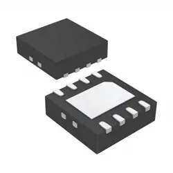
Bilder sind nur zur Referenz
S29GL01GS10TFI010
IC FLASH 1GBIT PARALLEL 56TSOP
- Hersteller
- Fr. Teil #S29GL01GS10TFI010
- Paket PG-TSOP-56
- Datenblatt
- Auf Lager5167
100% Original und Neu
24 Stunden bereit zum Versand
365 Tage Garantie
RFQ & Erhalten Sie mehr Rabatte
Spezifikationen
| Package | Tray |
| Series | GL-S |
| ProductStatus | Active |
| MemoryType | Non-Volatile |
| MemoryFormat | FLASH |
| Technology | FLASH - NOR |
| MemorySize | 1Gb (64M x 16) |
| MemoryInterface | Parallel |
| WriteCycleTime-WordPage | 60ns |
| AccessTime | 100 ns |
| Voltage-Supply | 2.7V ~ 3.6V |
| OperatingTemperature | -40°C ~ 85°C (TA) |
| MountingType | Surface Mount |
| Package/Case | 56-TFSOP (0.724, 18.40mm Width) |
Übersicht
Description
This memory type is commonly used in embedded systems, automotive applications, and consumer electronics due to its ability to execute code directly from Flash (XIP) and its endurance ratings of up to 100,000 program/erase cycles. The S29GL01GS10TFI010 supports multiple programming modes, including asynchronous and synchronous operations, and is available in various package types for flexibility in design. Its robust features make it suitable for applications needing long-term data retention and reliability.
Features
- Memory Density: 1 Gb (128 MB) capacity.
- Organization: 128M x 8 bits or 64M x 16 bits, allowing flexible data handling.
- Interface: Parallel interface for easy integration with various microcontrollers.
- Access Time: Offers fast read access times, typically around 100 ns.
- Sector Architecture: Supports multiple sectors (e.g., 64 KB sectors) for efficient memory management and data erasure.
- Erase Types: Supports sector, block, and chip erase functionalities.
- Endurance: Typically rated for 100,000 program/erase cycles per sector.
- Data Retention: Designed for a data retention period of up to 20 years.
- Voltage Range: Operates at a supply voltage of 2.7V to 3.6V.
These features make the S29GL01GS10TFI010 suitable for applications in consumer electronics, automotive, and industrial systems where reliable and fast memory is crucial.
Package
Pinout
Pin Count:
- 32 pins
Key Functions:
- Data I/O Pins: 8 data lines (DQ0 to DQ7) for data input and output.
- Address Pins: Used for addressing memory locations.
- Control Pins:
- CE (Chip Enable): Activates the device.
- OE (Output Enable): Enables data output.
- WE (Write Enable): Initiates write operations.
- RESET: Resets the device.
- Vcc and Vss: Power supply and ground connections.
This device supports various features such as uniform sector architecture, read, write, and erase functions, suitable for embedded applications.
Manufacturer
Application
Equivalent
Versand
VersandmethodenWir
bieten Sie globale Versanddienstleistungen durch DHL, FedEx, TNT, UPS oder einen anderen Spediteur Ihrer Wahl.
Versandgebührenreferenz (DHL/FedEx):
DHL: Versandkosten reichen von $25-$45 (0.5kg), mit einer geschätzten Lieferzeit von 2-5 Werktagen.
von FedEx: Versandkosten reichen von $25-$40 (0.5kg), mit einer geschätzten Lieferzeit von 3-7 Werktagen.
UPS: Versandkosten reichen von $25-$45 (0.5kg), mit einer geschätzten Lieferzeit von 3-7 Werktagen.
TNT: Versandkosten reichen von $25-$65 (0.5kg), mit einer geschätzten Lieferzeit von 3-7 Werktagen.
EMS: Versandkosten reichen von $30-$50 (0.5kg), mit einer geschätzten Lieferzeit von 7-15 Werktagen.
Registrierte Luftpost: Versandkosten sind $ 2- $ 4 (0,1 kg), mit einer geschätzten Lieferzeit von 5-20 Werktagen.
Zahlungen
Payment Methods
Die Zahlungsfrist ist 100% Prepaid.
Derzeit akzeptieren wir nur die folgenden Zahlungsmethoden:
1. PayPal
2. Kredit- / Debitkarte
3. Überweisung
Ähnliche
-
![MX25R8035FM1IL0]() MX25R8035FM1IL0
MX25R8035FM1IL0
Macronix
-
![MX25V1635FZNI]() MX25V1635FZNI
MX25V1635FZNI
Macronix
-
![MX66U1G45GXDI00]() MX66U1G45GXDI00
MX66U1G45GXDI00
Macronix
-
![MX25V2033FM1I]() MX25V2033FM1I
MX25V2033FM1I
Macronix
-
![MX25L8035EM2I-10G]() MX25L8035EM2I-10G
MX25L8035EM2I-10G
Macronix
-
![MX25L6433FM2I-08G]() MX25L6433FM2I-08G
MX25L6433FM2I-08G
Macronix
-
![MX25L12833FZ2I-10G]() MX25L12833FZ2I-10..
MX25L12833FZ2I-10..
Macronix
-
![MX25L12833FZNI-10G]() MX25L12833FZNI-10..
MX25L12833FZNI-10..
Macronix
-
![MX25L12835FZ2I-10G]() MX25L12835FZ2I-10..
MX25L12835FZ2I-10..
Macronix
-
![MX25L25645GXDI-08G]() MX25L25645GXDI-08..
MX25L25645GXDI-08..
Macronix
-
![MX30LF4G18AC-TI]() MX30LF4G18AC-TI
MX30LF4G18AC-TI
Macronix
-
![MX25U51245GZ4I00]() MX25U51245GZ4I00
MX25U51245GZ4I00
Macronix