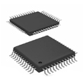
Bilder sind nur zur Referenz
S34ML01G200BHI000
IC FLASH 1GBIT PARALLEL 63BGA
- Hersteller
- Fr. Teil #S34ML01G200BHI000
- Paket 63-VFBGA
- Datenblatt
- Auf Lager3214
100% Original und Neu
24 Stunden bereit zum Versand
365 Tage Garantie
RFQ & Erhalten Sie mehr Rabatte
Spezifikationen
| Package | Tray |
| Series | ML-2 |
| ProductStatus | Active |
| MemoryType | Non-Volatile |
| MemoryFormat | FLASH |
| Technology | FLASH - NAND |
| MemorySize | 1Gb (128M x 8) |
| MemoryInterface | Parallel |
| WriteCycleTime-WordPage | 25ns |
| Voltage-Supply | 2.7V ~ 3.6V |
| OperatingTemperature | -40°C ~ 85°C (TA) |
| MountingType | Surface Mount |
| Package/Case | 63-VFBGA |
Übersicht
Description
Key features include a small form factor, low power consumption, and robust reliability, which make it ideal for mobile and portable devices. The S34ML01G200BHI000 is built to withstand a significant number of program/erase cycles and offers error correction capabilities, ensuring data integrity.
This NAND flash memory supports various modes of operation, including page read/write and block erase, catering to the needs of developers seeking flexible memory solutions. Overall, the S34ML01G200BHI000 represents a reliable choice for applications requiring efficient, high-density non-volatile memory.
Features
- Density: 1 Gbit (128 MB).
- Interface: Parallel interface, enabling high-speed data transfer.
- Access Time: Fast access times, typically around 70 ns.
- Voltage Range: Operates within a supply voltage range of 2.7V to 3.6V.
- Endurance: Supports a minimum of 100,000 program/erase cycles.
- Data Retention: Guaranteed data retention of 20 years.
- Package Options: Available in various packages, including 48-pin TSOP and 64-ball BGA.
- Compatibility: Ideal for a range of applications, including automotive, consumer electronics, and industrial systems.
- Program/Erase: Supports byte, page, and sector programming modes.
This device is well-suited for applications requiring reliable and high-density non-volatile memory.
Package
Pinout
The key functions of the pins include:
- Data Pins (DQ0-DQ7): Bidirectional data input/output for transferring data.
- Command Pins (CLE, ALE): For command and address latch enabling.
- Control Pins (WE, RE, CE): Control write, read, and chip enable operations.
- WP (Write Protect): Protection against unintended writes.
- RB (Ready/Busy): Indicates the readiness of the device for the next operation.
- VCC and VSS: Power supply and ground connections.
This device is used in various applications requiring non-volatile memory, such as smartphones, tablets, and embedded systems.
Manufacturer
Application
Equivalent
Versand
VersandmethodenWir
bieten Sie globale Versanddienstleistungen durch DHL, FedEx, TNT, UPS oder einen anderen Spediteur Ihrer Wahl.
Versandgebührenreferenz (DHL/FedEx):
DHL: Versandkosten reichen von $25-$45 (0.5kg), mit einer geschätzten Lieferzeit von 2-5 Werktagen.
von FedEx: Versandkosten reichen von $25-$40 (0.5kg), mit einer geschätzten Lieferzeit von 3-7 Werktagen.
UPS: Versandkosten reichen von $25-$45 (0.5kg), mit einer geschätzten Lieferzeit von 3-7 Werktagen.
TNT: Versandkosten reichen von $25-$65 (0.5kg), mit einer geschätzten Lieferzeit von 3-7 Werktagen.
EMS: Versandkosten reichen von $30-$50 (0.5kg), mit einer geschätzten Lieferzeit von 7-15 Werktagen.
Registrierte Luftpost: Versandkosten sind $ 2- $ 4 (0,1 kg), mit einer geschätzten Lieferzeit von 5-20 Werktagen.
Zahlungen
Payment Methods
Die Zahlungsfrist ist 100% Prepaid.
Derzeit akzeptieren wir nur die folgenden Zahlungsmethoden:
1. PayPal
2. Kredit- / Debitkarte
3. Überweisung
Ähnliche
-
![MX25R8035FM1IL0]() MX25R8035FM1IL0
Macronix
-
![MX25L3233FM1I-08Q]() MX25L3233FM1I-08Q
Macronix
-
![MX25V1635FZNQ03]() MX25V1635FZNQ03
Macronix
-
![MX29F400CBTI-70G]() MX29F400CBTI-70G
Macronix
-
![MX25V5126FM1I]() MX25V5126FM1I
Macronix
-
![MX25R3235FZNIL0]() MX25R3235FZNIL0
Macronix
-
![MX25L25673GMI-08G]() MX25L25673GMI-08G
Macronix
-
![MX25L25673GMI-10G]() MX25L25673GMI-10G
Macronix
-
![MX25U51279GXDR00]() MX25U51279GXDR00
Macronix
-
![MX25U25643GZNI00]() MX25U25643GZNI00
Macronix
-
![MX25L6433FM2I-08G]() MX25L6433FM2I-08G
Macronix
-
![MX25U25645GXDI00]() MX25U25645GXDI00
Macronix