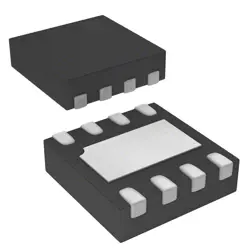
Bilder sind nur zur Referenz
SCANSTA112VS
IC INTERFACE SPECIALIZED 100TQFP
- Hersteller
- Fr. Teil #SCANSTA112VS
- Paket
- Datenblatt SCANSTA112VS DataSheet
- Auf Lager3893
100% Original und Neu
24 Stunden bereit zum Versand
365 Tage Garantie
RFQ & Erhalten Sie mehr Rabatte
Spezifikationen
| Part Status | Obsolete |
| Applications | Testing Equipment |
| Interface | IEEE 1149.1 |
| Voltage - Supply | 3V ~ 3.6V |
| Package / Case | 100-TQFP |
| Supplier Device Package | 100-TQFP (14x14) |
| Mounting Type | Surface Mount |
| Base Product Number | SCANSTA112 |
Übersicht
Description
Key features include advanced signal analysis capabilities, which help engineers identify and mitigate issues like crosstalk, reflection, and jitter. This functionality aids in optimizing circuit designs and ensuring compliance with industry standards. The SCANSTA112VS also offers a user-friendly interface, making it accessible to both novice and experienced engineers.
By utilizing this tool, designers can enhance the reliability and performance of their systems, reducing time-to-market and development costs. It is essential for engineers focused on maintaining signal quality in high-speed environments.
Features
1. Multi-Mode Testing: Supports both boundary scan and parallel test modes, enabling flexibility in testing strategies.
2. Test Access Port (TAP): Compliant with IEEE 1149.1 standards, ensuring standardized test access for easier integration.
3. Built-in Self-Test (BIST): Incorporates BIST capabilities, allowing for self-testing of the device without external test equipment.
4. Reduced Pin Count: Optimizes the number of test pins required, enhancing the overall design efficiency.
5. Fault Coverage: Provides high fault coverage through comprehensive scan capabilities, improving reliability.
6. Scalability: Easily scalable for various designs, accommodating different chip sizes and complexities.
7. Low Power Consumption: Designed to minimize power usage during testing, contributing to overall system efficiency.
These features make the SCANSTA112VS a robust solution for enhancing the testability and reliability of digital circuits.
Package
Pinout
Manufacturer
Application
Equivalent
Versand
VersandmethodenWir
bieten Sie globale Versanddienstleistungen durch DHL, FedEx, TNT, UPS oder einen anderen Spediteur Ihrer Wahl.
Versandgebührenreferenz (DHL/FedEx):
DHL: Versandkosten reichen von $25-$45 (0.5kg), mit einer geschätzten Lieferzeit von 2-5 Werktagen.
von FedEx: Versandkosten reichen von $25-$40 (0.5kg), mit einer geschätzten Lieferzeit von 3-7 Werktagen.
UPS: Versandkosten reichen von $25-$45 (0.5kg), mit einer geschätzten Lieferzeit von 3-7 Werktagen.
TNT: Versandkosten reichen von $25-$65 (0.5kg), mit einer geschätzten Lieferzeit von 3-7 Werktagen.
EMS: Versandkosten reichen von $30-$50 (0.5kg), mit einer geschätzten Lieferzeit von 7-15 Werktagen.
Registrierte Luftpost: Versandkosten sind $ 2- $ 4 (0,1 kg), mit einer geschätzten Lieferzeit von 5-20 Werktagen.
Zahlungen
Payment Methods
Die Zahlungsfrist ist 100% Prepaid.
Derzeit akzeptieren wir nur die folgenden Zahlungsmethoden:
1. PayPal
2. Kredit- / Debitkarte
3. Überweisung
Ähnliche
-
![MX25L3233FZBI-08Q]() MX25L3233FZBI-08Q
MX25L3233FZBI-08Q
Macronix
-
![MX25V1635FZNI]() MX25V1635FZNI
MX25V1635FZNI
Macronix
-
![MX25V1635FZNQ03]() MX25V1635FZNQ03
MX25V1635FZNQ03
Macronix
-
![MX25V16066M1I02]() MX25V16066M1I02
MX25V16066M1I02
Macronix
-
![MX29GL512FHXFI-11G]() MX29GL512FHXFI-11..
MX29GL512FHXFI-11..
Macronix
-
![MX25L2006EM1I-12G]() MX25L2006EM1I-12G
MX25L2006EM1I-12G
Macronix
-
![MX25R1635FZUIH0]() MX25R1635FZUIH0
MX25R1635FZUIH0
Macronix
-
![MX25L6433FM2I-08G]() MX25L6433FM2I-08G
MX25L6433FM2I-08G
Macronix
-
![MX29LV160DTTI-70G]() MX29LV160DTTI-70G
MX29LV160DTTI-70G
Macronix
-
![MX25L25645GXDI-08G]() MX25L25645GXDI-08..
MX25L25645GXDI-08..
Macronix
-
![MX29F800CBTI-70G]() MX29F800CBTI-70G
MX29F800CBTI-70G
Macronix
-
![MX25L1006EMI-10G]() MX25L1006EMI-10G
MX25L1006EMI-10G
Macronix